Linear regulator integrated circuits (ICs) step a voltage down from a higher voltage to a lower voltage without the need of an inductor. The low dropout (LDO) linear regulator is a special type of linear regulator in which the drop- out voltage—the differential between the input-to-output voltage needed to maintain regulation—is typically below 400 mV. Early linear regulator designs offered dropouts on the order of ~1.3 V, meaning for a 5 V input, the maximum achievable output was only ~3.7 V for the device to stay in regulation. Nevertheless, in these days of more sophisticated design techniques and wafer fabrication processes, the approximate definition of low is <100 mV to 300 mV or so.
Furthermore, although the LDO regulator is often one of the least costly components in any given system, it is often one of the most valuable components from a cost/benefit basis. In addition to output voltage regulation, another of the LDO regulator’s key tasks is to protect expensive downstream loads from harsh environmental conditions such as voltage transients, power supply noise, reverse voltage, current surges, etc. In short, its design must be robust and contain all the protection features needed to absorb the punishment from its environment while protecting the load. Many low cost LDO linear regulators do not have the necessary protec- tion features and thus fail, often causing damage not only to the regulator itself, but also the downstream load.
LDO Regulators vs. Other Regulators
Low voltage step-down conversion and regulation can be achieved via a variety of methods.
Switching regulators operate with high efficiency over a wide range of voltages but require external components such as inductors and capacitors for operation, thus taking up a relatively larger board area. Inductorless charge pumps (or switched capacitor voltage converters) can also be used to achieve lower voltage conversion and typically operate with higher efficiency depending on the conversion region, but are limited in output current capability, suffer from poor transient performance, and require more external components vs. those of a linear regulator.
Today’s generation of fast, higher current, low voltage digital ICs, such as FPGAs, DSPs, CPUs, GPUs, and ASICs, have placed more stringent demands on supplies that power the core and I/O channels. Traditionally, because charge pumps lack the necessary output current and transient response, efficient switching regulators have been used to power these devices. However, switchers have potential noise interference issues, and sometimes they have a slow transient response and layout limitations.
Thus, LDO regulators are an alternative in these applications, as well as other low voltage systems. Thanks to recent product innovations and feature enhancements, LDO regulators offer some performance benefits that make them more desirable.
Furthermore, when it comes to powering noise sensitive analog/ RF applications (commonly found in test and measurement systems, where the measurement accuracy of the machine or equipment needs to be orders of magnitude better than the entity being measured), LDO regulators are generally preferred over their switching counterparts. Low noise LDO regulators power a wide range of analog/RF designs,
including frequency synthesizers (PLLs/VCOs), RF mixers and modula- tors, high speed and high resolution data converters, and precision sensors. Nevertheless, these applications have reached sensitivities that are testing the limits of conventional low noise LDO regulators. For instance, in many high end VCOs, power supply noise directly affects the VCO output phase noise (jitter). Moreover, to meet overall system efficiency requirements, the LDO regulator usually postregulates the output of a relatively noisy switching converter, so the high frequency power supply ripple rejection (PSRR) performance of the LDO becomes paramount. Further, noise levels may be reduced by two to three orders of magnitude by an LDO regulator compared to a standard industry switch- ing regulator from the mV (rms) range to the single-digit μV (rms) range.
LDO Design Challenges
Some ICs, such as operational amplifiers and instrumentation amplifiers, plus data converters such as digital-to-analog converters (DACs) and analog-to-digital converters (ADCs), are referred to as dual polarity because they require two input supplies for power: one positive and one negative. The positive rail has typically been powered by a positive voltage reference or, even better, a linear or low dropout regulator. The negative rail was traditionally powered by a negative switching regulator or inverter. However, the inductor-based switcher can easily introduce noise into the system. With the advent of negative regulators, it has become advanta- geous to power the negative system rail with a negative LDO regulator and take advantage of all the LDO regulator features (no inductor, lower noise, higher PSRR, fast transient response, bulletproof protection). Older vintage LDO regulators have much worse PSRR and noise performance, and while they still can be used to create these types of quiet supplies, it takes a lot of extra components, board space, and design time to put a system together. These extra components also can adversely affect the power budget depending on their characteristics (parasitic resistance, etc.).
There is another difficult system performance characteristic for custom- ers using an op amp, ADC, or other signal chain component: these ICs do not have infinite supply rejection capability and, worse, the supply rejec- tion capability can be significantly lower at high frequency. In the past, this has meant using extra filtering components on the board, which increases solution size. Further, if a designer is trying to obtain higher accuracy, more trouble may result if the regulator supply has excessive noise, which causes unwanted variation in a measurement scenario.
Plenty of industry-standard linear regulators perform the low dropout operation with a single voltage supply, yet most cannot achieve the combination of very low voltage conversion with low output noise, wide ranging input/output voltages, and extensive protection features. PMOS LDO regulators achieve the dropout and run on a single supply but are limited at low input voltages by the pass transistor’s VGS characteristics and they lack the many protection features from high performance regula- tors. NMOS-based devices offer a fast transient response but require two supplies to bias the device. NPN regulators offer a wide input and output voltage range, but they require two supply voltages or have higher dropout. By contrast, with the proper design architecture, a PNP regulator can achieve low dropout, high input voltage, low noise, high PSRR, and very low voltage conversion with bulletproof protection and all from a single-supply rail. For best overall efficiency, many high performance analog and RF circuits are powered from LDO regulators postregulating the output of a switching converter. This requires high PSRR and low output voltage noise at low input-to-output differentials across the LDO regulator. An LDO regulator with high PSRR easily filters and rejects noise from the switcher’s output without requiring bulky filtering components. Further, a device with low output voltage noise across a wide bandwidth is beneficial for today’s modern rails where noise sensitivity is a key consideration. Low output voltage noise at high currents is clearly a must-have specification.
New Ultralow Noise, Ultrahigh PSRR LDO Regulators
It’s clear that an LDO solution that solves the issues outlined herein should have the following attributes:
- Very low output noise
- High PSRR across a broad range of frequencies
- Low dropout operation
- Single-supply operation (for ease of use and relaxed supply sequencing challenges)
- Fast transient response time
- Operation over a wide input/output voltage range
- Moderate output current capability
- Excellent thermal performance
- Compact footprint
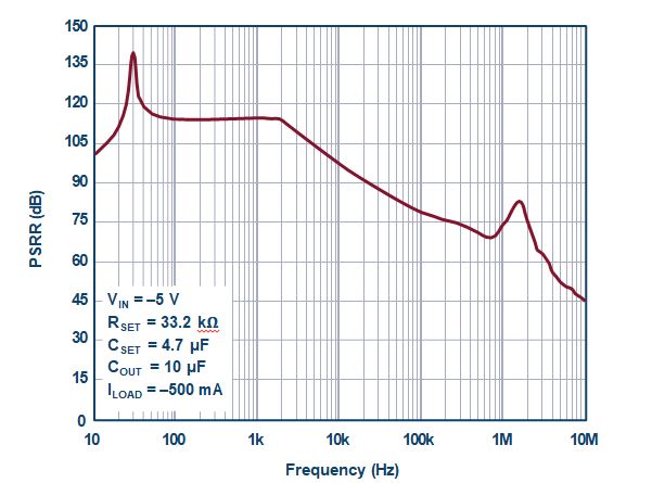
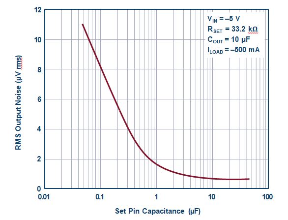
To address these specific needs, Analog Devices introduced its LT304x family of ultrahigh PSRR, ultralow noise positive LDO regulators. The newest member is the complementary LT3094, an ultralow noise, ultrahigh PSRR low dropout voltage 500 mA negative linear regulator. This device is a negative version of the popular 500 mA LT3045 (LT3042 for 200 mA). The LT3094’s unique design features ultralow spot noise of only 2 nV/√Hz at 10 kHz and 0.85 µV rms integrated output noise across a wide 10 Hz to 100 kHz bandwidth. PSRR performance is excep- tional: low frequency PSRR exceeds 100 dB out to nearly 4 kHz and high frequency PSRR exceeds 70 dB out to 2 MHz, quieting noisy or high
ripple input supplies. The LT3094 utilizes a proprietary LDO architecture: a precision current source reference followed by a high performance unity-gain buffer, which results in virtually constant bandwidth, noise, PSRR, and load regulation performance, independent of output voltage. In addition, this architecture permits paralleling of multiple LT3094s to further decrease noise, increase output current, and spread heat on a printed circuit board.
The LT3094 delivers up to 500 mA output current with a 230 mV dropout voltage at full load, across a wide –2 V to –20 V input voltage range. The output voltage range is 0 V to –19.5 V and the output voltage tolerance is highly accurate at ±2% over line, load, and temperature. The device’s wide input and output voltage ranges, high bandwidth, high PSRR, and ultralow noise performance are ideal for powering noise sensitive applications such as PLLs, VCOs, mixers, and LNAs; very low noise instrumentation such as test and measurement, and high speed/high precision data converters; medical applications such as imaging and diagnostics, and precision power supplies; and postregulators for switching power supplies. The LT3094 operates with a small, low cost, 10 µF ceramic output capaci- tor that optimizes stability and the transient response. A single resistor programs the external precision current limit (±10% overtemperature). The device’s VIOC pin controls an upstream regulator to minimize power dissipation and optimize PSRR. A single SET pin capacitor lowers output noise and provides reference soft start functionality, preventing output voltage overshoot at turn-on. Moreover, the device’s internal protection circuitry includes internal current limit with foldback and thermal limit with hysteresis. Other features include fast start-up capability (useful if a large value SET pin capacitor is used) and a power good flag (the industry’s first negative LDO regulator with this function) with a programmable threshold to indicate output voltage regulation.
The LT3094 is available in thermally enhanced 12-lead, 3 mm × 3 mm DFN and MSOP packages, both with a compact footprint. The E- and I-grade versions are available from stock with an operating junction temperature of –40°C to +125°C.
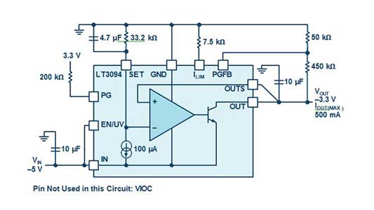
The LT3094 requires an output capacitor for stability. Given its high band- width, it is recommended to use low ESR and ESL ceramic capacitors. A minimum 10 µF output capacitance with an ESR below 30 mΩ and an ESL below 1.5 nH is required for stability. Given the high PSRR and low noise performance attained with using a single 10 µF ceramic output capacitor, larger values of output capacitor only marginally improve the performance because the regulator bandwidth decreases with increasing output capacitance—hence, there is little to be gained by using larger than the minimum 10 µF output capacitor. Nonetheless, larger values of output capacitance do decrease peak output deviations during a load transient.
Benefits of Parallel Devices
Higher output current is obtained by paralleling multiple LT3094s. Tie all SET pins together and all IN pins together. Connect the OUT pins together using small pieces of PCB trace (used as a ballast resistor) to equalize currents in the LT3094. More than two LT3094s can also be paralleled for even higher output current and lower output noise. The output noise decrease is proportional to the square-root of the number of devices in parallel. Paralleling multiple LT3094s is also useful for distributing heat on the PCB. For applications with a high input-to-output voltage differential, an input series resistor or resistor in parallel with the LT3094 can also be used to spread heat. See Figure 4 for a parallel circuit implementation.
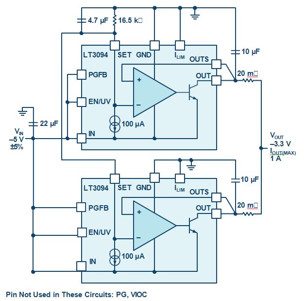
Table 1 shows the members of ADI’s ultrahigh PSRR, ultralow noise family of LDO regulators.

Conclusion
The positive 200 mA LT3042, 500 mA LT3045, and, now, the new comple- mentary LT3094 negative 500 mA LDO offer breakthrough noise and PSRR performance. These attributes, coupled with their wide voltage range, low dropout voltage, extensive protection features/robustness, and ease of use, make them ideal for powering noise sensitive bipolar positive/negative rails in test and measurement or medical imaging systems, for example. With their current reference-based architecture, noise and PSRR performance remain independent of the output voltage. Additionally, multiple devices can be directly paralleled to further reduce output noise, increase output current and spread heat on the PCB. The LT3042, LT3045, and LT3094 save time and cost while improving application performance.
About the Author
Steve Knoth is a senior product marketing engineer in Analog Devices’ Power by Linear Group. He is responsible for all power management integrated circuit (PMIC) products, low dropout (LDO) regulators, battery chargers, charge pumps, charge pump-based LED drivers, supercapacitor chargers, low voltage monolithic switching regulators, and ideal diode
devices. Prior to joining Linear Technology (now ADI) in 2004, Steve held various marketing and product engineering positions since 1990 at Micro Power Systems, Analog Devices, and Micrel Semiconductor. He earned his bachelor’s degree in electri- cal engineering in 1988 and a master’s degree in physics in 1995, both from San Jose State University. Steve also received an M.B.A. in technology management from the University of Phoenix in 2000. In addition to enjoying time with his kids, Steve can be found tinkering with pinball/arcade games or muscle cars, and buying, selling, and collecting vintage toys and movie/sports/automotive memorabilia. He can be reached at steve.knoth@analog.com.


