Abstract
There has long been a desire for the capability of a wide 2 GHz to 18 GHz observa- tion bandwidth across a single Nyquist in electronic warfare (EW) and communi- cation intelligence (COMINT) systems. Interleaving ADC cores is an option to gain that capability, but it requires a front-end analog bandwidth of 2 GHz to 18 GHz. Time interleaving is a popular method to double the sample rate. However, there can be trade-offs with the challenge of processing large raw data rates and the capability to digitally filter within the ADC.
Introduction
challenges and possible approaches. Part 2 describes direct quadrature sampling in detail, along with measured results. Part 3 compares the quadrature results with time interleaving, enabling users to select the optimum choice based on their system objectives.
To double the Nyquist bandwidth of an ADC receiver, a traditional time interleav- ing method is often used. However, alternate architectures offer further advan- tages. In this 3-part series, we describe options for first Nyquist direct sampling of a 2 GHz to 18 GHz bandwidth using commercial ADCs. Part 1 introduces the
Part 1: Applications, Interleaving Basics, and AD9084 Options
The Aliasing Problem
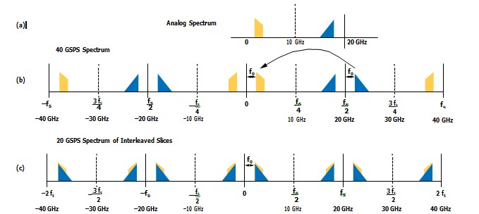
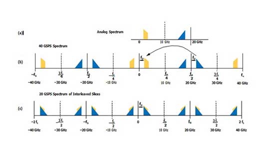
In Figure 1a, an analog spectrum is shown with a yellow desired signal in Nyquist zone 1 (0 – fS/2) and a blue blocker signal in Nyquist zone 2 (fS/2 – fS). According to the sampling theorem, digitally sampled analog signals will appear at integer multiples of fS. As shown in Figure 1b, both the narrow-band blocker and desired signals are copied at positive and negative integer multiples of fS. The architec- tural ADC challenge is how the system engineer can mitigate this known issue using alternate methods of sampling.

The Nyquist theorem states that undesirable aliasing effects occur when the sig- nal bandwidth is greater than fS/2. In sampled systems, the unique spectrum will only be visible from 0 to fS/2. Higher order Nyquist signals will alias or fold back into the Nyquist zone (0 to fS/2) as shown in Figure 1c in the form of undesired images. The image signals generated from frequencies greater than fS/2 will become blockers for the desired signals, lowering SFDR and sometimes rendering a signal unrecoverable.

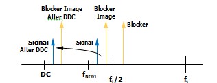
Figure 2. Spectral view of a blocker in the second Nyquist aliasing near a smaller first Nyquist signal of interest.
In traditional EW and COMINT systems, where blockers are present in higher order Nyquist zones, antialiasing (AA) filters are used. In first Nyquist sampling, low- pass filters are used to reject blockers above fS/2 and prevent their images from folding back into the first Nyquist. These systems work well if the desired signal is always in the first Nyquist zone. However, this will be directly dictated by the sample rate.
This setup is ineffective when the interfering signal is just above half the sam- pling frequency (fS/2), and the target signal is just below fS/2. In Figure 2, the interfering signal is too near to apply an AA filter without risking the loss of some of the desired bandwidth. A recommended practice is to use a 20% frequency guard band around fS/2.
A popular alternative to first Nyquist sampling is under-sampling, placing the desired signal bandwidth into a higher ADC Nyquist zone. In this case, the desired signal is in a higher order band greater than fS/2. The AA filter would practically be a band-pass filter (BPF) that surrounds the desired signal in the higher order band. This BPF rejects frequencies outside the pass band, which could be either a blocker or any out-of-band noise.
Interleaving
Time Interleaving—Full-Rate Offload
Traditional time interleaving of two or more ADCs with delayed clocks comes with both a benefit and trade-off. When two cores are used to simultaneously sample a signal with a sample rate of fS, then the resultant sample rate is simply 2 × fS. The ADCs must have a fixed clock phase relationship for the interleaving to work properly. The clock phase relationship is governed by Equation 1, where n is the specific ADC and m is the total number of ADCs.

For a dual ADC interleaving relationship, the sample clocks for each channel need to be 180° out of phase or alternately sampled on positive and negative edges of a clock that has an ideal 50% duty cycle. These can be challenging timing speci- fications to meet using external clocking solutions without introducing new inter- leaving artifacts. Additionally, the front-end RF splitter would need ideal characteristics for amplitude and phase matching; otherwise, unwanted spurious frequency power can be introduced at the fS/2 slice sample rate.
Depending upon how the back-end digital processing is used, a full-rate bitstream may be undesirable unless the total interleaved fS/2 Nyquist bandwidth can be used for the signals of interest. Some interleaving architectures may limit the dynamic range to 8 bits of a higher resolution converter.
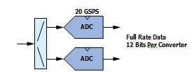
In this case, there would be no back-end digital corrections for small variances in the ADC channels such as offset, gain, and phase delay. Therefore, these mis- matches would be seen as interleaving artifacts within the Nyquist frequency spec- trum. They would diminish the usable dynamic range of the interleaved converter channel with unwanted images. Using the Analog Devices Apollo MxFE™ AD9084, there are two options that take advantage of a full rate offload. Figure 3 shows a single 12-bit pair of interleaved ADCs while Figure 4 shows two pairs of interleaved ADCs. To achieve the outputs of two channels, the bit resolution is reduced to 8 bits per sample.


Direct Quadrature Sampling Overview
Direct quadrature sampling is an alternate form of interleaving. The most widely used ping-pong interleaving method involves sequentially clocking two neighbor- ing ADCs. This is typically done by either doubling the clock frequency or sampling on both the rising and falling edges of the input clock. Quadrature interleaving does not invert the clock phase, but rather clocks two ADCs simultaneously with a common in-phase clock. A 90° phase shift of the RF input provides the informa- tion needed to resolve multiple Nyquist zones and double the effective sampling rate. This offers the advantage that post-ADC processing doesn’t need to double the sample rate.
In practice, the 90° phase shift is accomplished with a hybrid coupler, often referred to as a hybrid splitter. Wideband hybrid couplers are now available that cover a wide 2 GHz to 18 GHz bandwidth. However, a well-known issue in quadra- ture sampling is that any phase or amplitude mismatch in the I/Q balance creates unwanted perceived energy at the image frequency. The effect of this mismatch is not balanced as the differences between the two signals are magnified the larger the imbalances become. This creates a primary image interleaving spur at fS ± fIN due to the gain and phase mismatch between the I and Q signals.
Commercial hybrid couplers have historically only supported narrow bandwidths for smaller frequency targets. Wideband performance specifications are still maturing. With the introduction of wideband hybrid couplers from 2 GHz to 18 GHz, the matching performance is moderate as it is feasible to achieve a minimum of a few dB of amplitude error matching and several degrees of phase error matching across their bandwidth. The practical interleaving image spur power using only a hardware quadrature is –20 dBc at best. This is simply an unacceptable technical solution for most modern applications. Therefore, relying exclusively on a hardware solution for this type of interleaving will not be sufficient. A back-end quadrature error correction (QEC) matching algorithm in digital processing will be required to achieve SFDR performance of –50 dBc or better across a wide bandwidth.

Interleaving Options Using the AD9084 DSP
The AD9084 is a 4T4R RF sampling converter with an RF input bandwidth of 18 GHz. Figure 5 shows the ADCs and embedded DSP for half of the ADCs integrated into the IC.1 To prevent requiring a full-rate data offload, interleaving options were developed for both time and quadrature interleaving that maintain the use of the embedded DSP. This enables monitoring a full 2 GHz to 18 GHz bandwidth while still decimating to a lower rate to reduce digital payload and power in the adjacent digital chips.
Direct Quadrature Sampling: PFILT QEC
Quadrature interleaving uses two ADC cores by splitting the RF input signal in the hardware into 0° and 90° phases. Processing the signals separately is done as if the two signals are in ideal perfect quadrature. Unfortunately, the two split signals are not ideal due to significant mismatch in both phase and amplitude, which are common in current hardware hybrid performance. However, a back-end quadra- ture error correction algorithm can compensate for both the amplitude and phase mismatch between the two signals.
After a training signal is used to establish correction coefficients across the bandwidth (BW) of interest, the image spur of the quadrature sampling archi- tecture can be mitigated to better than –50 dBc using digital filter processing techniques. This maintains a consistent SFDR without the undesirable artifacts of 8× sub-ADC time interleaving found in numerous high speed architectures.

Direct Quadrature Sampling: CFIR QEC
A variation of the quadrature interleaving principle enables digital signal filtering before the QEC correction block in the complex FIR (CFIR). The SFDR performance in this case is generally improved since lower frequency ripple mismatch between the two channels can be corrected more easily with a longer processing latency. The numerically controlled oscillator (NCO) frequencies between the two DDCs are not set to be equal, but rather NCO2 = fS – NCO1. The reason for this NCO frequency difference is detailed in Part 2 of this article series. The 32-bit digital resolution accuracy of each NCO tuning word ensures that there is not any residual fre- quency mismatch between the DDCs that would contribute to unwanted spurious performance. A back-end summation step melds two channels into one with the cancellation of the first or second Nyquist.

Time Interleaving with PFILT or CFIR Error Correction
The same interleaving principles mentioned for quadrature can also be applied to the traditional time interleaving methods using internal inverted sample clocks. Instead of using a front-end quadrature hybrid, a true splitter would be used for time interleaving to multiple channels with back-end error correction. Each signal would be corrected with digital filtering coefficients. After filtering, two channels of decimated data would be output that would need to be re-assembled with digi- tal signal processing techniques.

Two time interleaving options have been evaluated using the embedded DSP. Figure 8 shows the time interleaving with the PFILT correction and Figure 9 shows the time interleaving configuration with the CFIR correction.

Additional Interleaving Considerations
Mismatch
Interleaving multiple ADCs presents challenges, including the appearance of spurious frequency power (spurs) in the output spectrum due to imperfect nonide- alities in each ADC core. These imperfections primarily arise from mismatches between the interleaved ADCs, notably in gain and phase or timing.
Small manufacturing variances, even for two adjacent ADCs on the same silicon, can cause enough gain variation to introduce a gain mismatch spur. In the case of the gain mismatch, there is no viable way to measure the gain mismatch unless a signal is presented to both ADCs to be measured. The gain mismatch will result in a spur in the output spectrum related to the input frequency and sampling rate. The spur will appear at fS – fIN.
To minimize the spur caused by the gain mismatch, a correction strategy to mitigate the mismatch is employed. The gain of one of the ADCs is chosen as the reference, and the gain of the other ADC is set to match that gain value as closely as possible. The more accurately that the gain values of each ADC are matched to each other, the less the resulting spur will be in the output spectrum.
Heavy Interleaving
Certain commercial architectures employ extensive sequential interleaving, utiliz- ing 8× ADC slices or more to expand the Nyquist bandwidth. For example, an 8-way interleaving would create interleaving spurs at frequencies of fS/8, fS/4, 3fS/8, and so forth. This would create a non-normal distribution of the noise spectral density (NSD) with interleaving spurs around the eight ADC slices. Without proper calibration to suppress these spurious frequencies, a sophisticated table or spur calculator tool to navigate interleaving artifacts quickly becomes unmanageable.
Conclusion
In Part 1 of this article series, we introduced a new method for direct sampling from 2 GHz to 18 GHz. From electronic warfare to communications intelligence, there are numerous cases where continuous monitoring of 2 GHz to 18 GHz is required. Without the need for specific AA filters, systems can resolve signals from multiple Nyquist zones. With careful quadrature error correction techniques of time or quadrature interleaved adjacent ADCs, systems can effectively double the sampling rate of a given digitizer. Using the hardened DSP functionality of the Apollo MxFE device, FPGA resources can be minimized and still monitor a full 2 GHz to 18 GHz spectrum all in one Nyquist.
Six options have been introduced with detailed descriptions coming in Part 2 and Part 3.
- Full rate offload, interleave ADCs on opposite sides
- Full rate offload, interleave adjacent ADCs
- Direct quadrature sampling: error correction with PFILT
- Direct quadrature sampling: error correction with CFIR
- Time interleaving: error correction with PFILT
- Time interleaving: error correction with CFIR
References
- 1Gabriele Manganaro. “Advanced Data Converters.” Cambridge University Press, 2012.
- Kester, Walt. “Analog-Digital Conversion.” Analog Devices, Inc., 2004. Ali, Ahmed. High Speed Data Converters. IET, 2016.
- Harris, Jonathan. “The ABCs of Interleaving ADCs.” Analog Devices, Inc., 2019.
- Manganaro, Gabriele and Robertson, David. “Interleaving ADCs: Unraveling the Mysteries.” Analog Dialogue, Vol. 49, July 2015.
About the Authors
Ian Beavers is a field applications engineer and customer labs manager for the Aerospace and Defense Systems team located at Analog Devices, Durham, North Carolina. He has worked for the company since 1999. Ian has over 25 years of experience in the semiconductor industry. Ian earned a bachelor’s degree in electrical engineering from North Carolina State University and an M.B.A. degree from the University of North Carolina at Greensboro.
Peter Delos is a technical lead in the Aerospace and Defense Group at Analog Devices in Greensboro, North Carolina. He received his B.S.E.E. degree from Virginia Tech in 1990 and M.S.E.E. degree from NJIT in 2004. Peter has over 30 years of industry experience. Most of his career has been spent designing advanced RF/analog systems at the architecture level, PWB level, and IC level. He is currently focused on miniaturizing high performance receiver, waveform generator, and synthesizer designs for phased array applications.
Brian Reggiannini is a senior principal engineer in system design. He has designed, implemented, and supported system-level calibrations for several generations of Analog Devices’ wireless transceiver products. His technical interests include signal processing, machine learning, embed- ded systems, and systems involving digitally assisted analog components. Brian earned Sc.B., Sc.M., and Ph.D. degrees from Brown University in 2007, 2009, and 2012, respectively.
Connor Bryant is a system applications engineer at Analog Devices working in the Aerospace and Defense Business Unit in Durham, North Carolina. He joined ADI in 2023. He is currently focused on RF mixed-signal chain design and analysis. He received his B.S.E.E degree from NC State University in 2022 and his M.S.E.E degree from NC State University in 2023.


