Easy Tactile Switch Integration
With the increasing availability of 3D files from manufacturers, placing the various electronic components on a PCB is relatively easy.
It becomes more complicated when integrating electromechanical components such as switches.
Their static installation is just as easy as any other electronic component. Still, it becomes more challenging when the switch forms an integral part of the Human-Machine Interface and requires a perfectly controlled mechanical actuation. This requirement is further complicated when considering that switches can be operated directly by a finger on a button or by levers or toggles.
The total of the tolerance stack must be calculated to guarantee the the switch’s actuation in all circumstances and its possible protection from overload and/or overtravel.
In general, two crieteria are specified by the manufacturers to allow the integration of the switch:
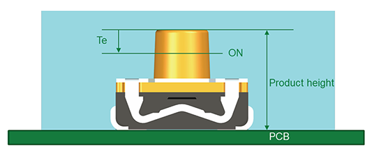
Electrical Travel (Te)

The Electrical Travel (Te) ON is defined as the travel of the acutator’s top which is required to reach the electrical switching point (ON).
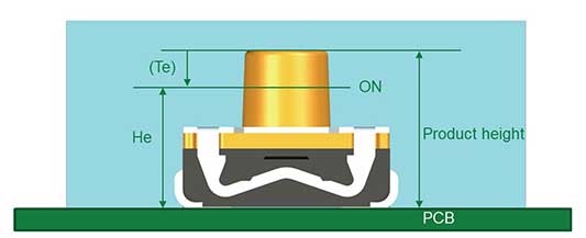
Electrical Height (He)

The Electrical Height (He) ON is defined as the product height when the electrical switching point (ON) is reached. The PCB is used as a reference, considering switch terminals in contact with the PCB (no solder thickness).
In most cases, the designer will use Electrical Travel, a stack-up analysis, to calculate the position of the electrical switching point using the top of the PCB as a reference. This method has the disadvantage of cumulating the tolerances of each of the criteria; therefore, it is very common to obtain tolerances of ±0.4 mm.
It needs to be confirmed that the actuator travel is always long enough to ensure electrical contact, which will expose the switch to significant over-travel. Since the position of the switch point could be more precise, the travel and tactile effect in the application will be proportionally affected and could provide a poor overall feel.
Replacing Electrical Travel with Electrical Height
C&K, now part of Littelfuse, redesigned the product’s functional dimensions to facilitate integration and provide even more support to customers. The product itself and its behaviour remained unchanged but the electrical switching position from the PCB is now consistently specified with better accuracy due to extensive process controls and improved manufacturing methodologies.
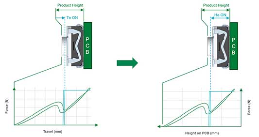
A comparison: Electrical Travel and Electrical Height

Figure 5: Now: Electrical Height He ON
Figure 4: Previously: Electrical Travel Te ON
Numerical approach:
- Product height = 3.5+/-0.2mm
- Te ON = 0.5+/-0.2mm
- Equivalent Electrical Height is usually calculated He ON eq = 3.0+/-0.4mm
Figure 5: Now: Electrical Height He ON
Specification:
- Product height = 3.5+/-0.2mm
- He ON = 3.0+/-0.2mm
Advantages of the Electrical Height
- As a general manner, tolerances on:
- Product height is ±0.2 mm
- Electrical travels are ±0.2 mm (can be ±0.25 mm or ±0.3 mm for high actuation forces).
- In general, designers need to know the switching point position from the PCB and apply the formula:
- Product Height ±0.2 mm – Electrical travel ±0.2 mm = Equivalent Electrical Height He ±0.4 mm as a minimum tolerance.
- The target of replacing the Electrical Travel (Te) value by the Electrical Height (He) is to avoid cumulated tolerances and to propose a functional characteristic with a tighter tolerance.
- Electrical Height (He) is stable , with a standard tolerance of ±0.2 mm. C&K can develop KSC versions on request with exact tolerances on such dimension: ±0.1 mm or ±0.08 mm.
- Only J terminals are recommended for He versions. No change for G terminals.
- In the same way, Mechanical Travel is replaced by the Mechanical Height.
- Please note that nominal values for both electrical and mechanical travel are still provided within the specifications for information.


