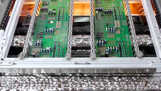
Electronics manufacturers face more challenges than ever if they want to succeed in a highly competitive environment. On the one hand, the requirement for consistently high quality of the manufactured products dominates, which often requires a certain degree of flexibility in the manufacturing processes. On the other hand, there is price pressure and the overall goal of making manufacturing processes more sustainable in order to be well positioned for the future. The focus is on minimizing material waste, the economical and ecological use of resources and avoiding potential soldering errors.
Machine manufacturers can provide effective support in the transformation to sustainable electronics production. More energy-efficient and resource-saving systems, increasing the flexibility of production equipment in order to be able to react economically to production fluctuations, higher levels of automation in process control in order to avoid possible soldering errors and of course the optimization of the overall cost structure are some of the starting points. Often, it’s the little things that make a difference.
Avoid Waste
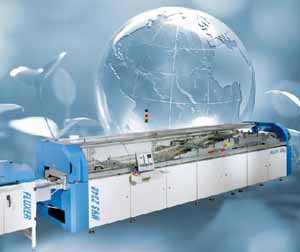
When it comes to minimizing the generation of waste in wave soldering processes, it is worth considering a nitrogen atmosphere. The less oxygen is present in the process, the lower the oxide formation in the solder bath, and what does not have to be removed as “waste” in the form of oxides therefore does not have to be reintroduced as fresh solder. Around 30 kg of oxides, which are produced in 3-shift operation in an open system, are reduced to just 5 kg in a nitrogen tunnel system. At the same time, machine availability is also significantly higher, as the cleaning effort is reduced as well.
A nitrogen atmosphere also has a positive effect on flux consumption. The main task of the flux is to remove oxide and polymer layers from the metal surfaces and to protect against new oxidation. A large part of the flux is washed off as the board passes through the first wave, but the solder joint is formed directly after passing through the second wave and the peel-off behavior is decisive for its shape. Inert conditions ensure improved wetting properties and a lower surface tension of the liquid solder. Reoxidation of the metallized surfaces is prevented and the “on-top quantity” of flux required to remove metal oxides in an ambient atmosphere can be saved in a nitrogen atmosphere.
The use of nitrogen in soldering processes naturally results in costs, which leads directly to the question of how nitrogen consumption can be reduced to the minimum required level. Modern systems can be equipped with an automatic control system that ensures a constantly stable nitrogen atmosphere and prevents N2 consumption from drifting unnoticed, for example due to asymmetrical flows in the tunnel.
Smart functions, such as an ECO mode, also help to implement a more sustainable soldering process cost-effectively and enable savings of up to 20%. With an ECO mode, the nitrogen supply is automatically reduced if no assemblies are currently being processed. Depending on the individual production requirements, a system can be programmed to automatically reduce the N2 supply after x minutes of inactivity or, for example, only at fixed pause times.
Utilize Potential
Significant resource savings are possible in the fluxer area, regardless of whether the wave soldering system is operated in a nitrogen atmosphere or not.
A modern spray head with a stable spray jet ensures greater utilization of the flux. Less spray mist is produced, which minimizes the level of contamination in the system. This results in cost savings on both sides. Flux consumption can be reduced by up to 30 % with a modern HVLP spray head (high volume – low pressure) compared to a normal spray head.

Monitoring the amount of flux applied offers further potential for savings: Deviations from the target value are detected very early and the cause, such as contamination or deposits, defective hoses, or wear, can be rectified quickly. The frequently set “reserve quantity” for flux application can be omitted.
In wave soldering processes, the flux is usually applied to the entire assembly, even if not all areas are actually soldered. With the smart function of segmented flux application, it is possible to flux only those areas of the assembly where solder joints are present. Up to eight different areas can be defined within an assembly, each segment with a minimum size of 50 x 50 mm. Depending on the assembly layout, the potential savings can quickly amount to 50% or more.
Soldering = Heat and Heat = Energy
The energy sector offers by far the greatest potential for savings, and there are several starting points here.
When heating up a soldering system, load peaks generally occur which have a high energy requirement. The savings potential is correspondingly high if these load peaks are avoided. With an ECO mode, the preheating zones are controlled and heated separately from each other until the system is fully operational. This optimized heating mode can reduce the energy requirement by up to 30 %.
Around 70 % of the energy consumption of a wave soldering system is required for the preheating process. A system with a total connected load of 38 kW, equipped with infrared and quartz radiators in the preheating area, settles at an average consumption of approx. 14 kW during operation. If the preheating is switched off, the energy consumption drops to approx. 4 kW while the solder bath temperature remains constant at 260°C. From the process side, it is not possible to do without preheating the assemblies. Conversely, solutions are needed to reduce the energy requirement in the preheating process while maintaining at least a constant production output.
Several machine states play a role in determining the energy efficiency of a soldering system:
- Switched off: No energy consumption, but it takes a certain amount of time before the system is ready for use again.
- Standby: The machine only needs a short time to be in operation mode again.
- Variable load: fewer products enter the system than it could process.
- 100 % load: The machine produces at maximum throughput.
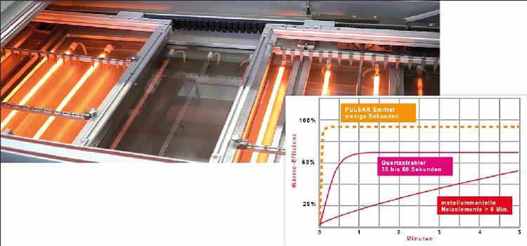
Let’s first take a look at three different types of emitters. Quartz emitters are a common preheating method in the soldering process, but only achieve an average heating efficiency of 60-70 %, metal-coated emitters even less. Pulsar radiators emit more than 85 % of the total power in infrared heat and are therefore significantly more effective. Apart from that, they are at full power within a few seconds, while other types of emitters require a certain start-up time.
If you look at the wave range in which the different types of radiators operate, pulsar emitters are in the medium wave range. They therefore have a greater penetration depth than quartz radiators, which makes them more efficient in terms of heat transfer.
Compared to quartz radiators, pulsar emitters can therefore achieve savings of up to 10 %. In relation to infrared heaters, energy savings of up to 30 % can be achieved through precise timing.
All in all, pulsar heaters have a higher heating efficiency, a shorter response time and a better heat input into the product compared to quartz emitters.
If the different machine states already mentioned are considered, pulsar heaters can significantly reduce the energy consumption of the soldering system. If the machine is empty and switched to standby mode, the heaters can be set to a minimum, as it only takes seconds for the heat output to return to within the working range. Only approx. 3.5 kW is required to keep the ambient conditions in the system constant.
If the production volume is less than 100 %, all radiators above which is currently no product, can be switched to their standby setting. A low load is therefore also directly associated with lower energy consumption. With low machine utilization up to 50 % simply by minimizing standby consumption.
At 100 % load, the power consumption of the system is almost identical to the power consumption of a machine with conventional radiators.
One of the main advantages of pulsar heaters is the fast regulation speed. No waiting time is required between products, either in series production or in a product mix with different thermal requirements. By switching individual radiators instead of entire heating segments, the shortest possible assembly distances are possible. In practice, this means that each individual emitter below a product can be operated with the individually required settings and no additional distance between different products is required to achieve this individual setting value. As a result, this creates enormous flexibility and maximum throughput.
Avoid Soldering Defects
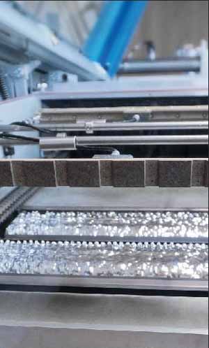
Soldering defects are not only annoying, but above all time-consuming and costly. At best, they require additional process steps and rework, and therefore unnecessary use of energy, materials, and personnel. In the worst case, the product is scrap.
The most common soldering faults include defects due to poor wetting, especially if the assembly or mask layout is demanding. Depending on the mask thickness and size of the mask cut-outs, reliable wetting of all solder joints is not always guaranteed. In addition, small distances between the covered components and the pins of the components to be soldered can become a challenge. Incomplete solder joints, missing through-hole penetration or solder bridges are then classic defects.
Smart functions such as the automatic nozzle height adjustment are an innovative approach to such challenges. The solder nozzles can be adjusted individually and software-controlled over a distance of 20 mm in order to always have the optimum distance between the PCB and solder nozzle, depending on the product, in up to 16 different sections of a PCB.
This makes the entire process independent of the workpiece carrier or assembly design, without affecting the cycle time. All solder joints can be reliably wetted, remarkably reducing the risk of soldering defects. At the same time, the automatic nozzle height adjustment offers maximum flexibility and thus ensures the future viability of the wave soldering system with regard to new applications.
The stable height of the solder wave is also relevant to the process. Poor penetration or insufficient wetting can be the result of an irregular wave height, which is why it has long been automatically monitored and controlled in selective soldering processes.
There are also methods for wave soldering processes, but they are all associated with limitations: The wave height is not measured across the entire width, production has to be interrupted or it is not possible to draw conclusions about individual production.
SEHO has developed the automatic wave height measurement with a focus on precisely this aspect. The system is based on contact measurement across the entire wave width, which ensures reliable results and processes for both laminar and turbulent solder waves and does not affect the cycle time of the wave soldering system.
To determine the ideal state of the wave height, a reference measurement is first carried out. In production mode, the height of the wave is then measured automatically in a programmable time grid. Based on these measurement results and a mathematical model, the wave height is automatically regulated within adjustable tolerances. All measurement results and readjusted parameters are of course documented for complete traceability.

The advantages are obvious: process deviations are detected at an early stage and the cause can be quickly analyzed and rectified. This ensures high product quality and production costs are sustainably reduced by avoiding rework or scrap.
Conclusion
Making the manufacture of electronic products more sustainable for the future is one of the primary goals today. Modernization and smart machine functions not only increase energy and resource efficiency, but also enable more environmentally friendly production processes. With the right strategy, the modern, sustainable orientation of the soldering process can lead to long-term cost optimization while minimizing the ecological footprint.


