Abstract
This article introduces the replacement of PhotoMOS® switches with CMOS switches in automated test equipment (ATE) houses. The CMOS switches not only match the performance benefits of PhotoMOS in terms of capacitance-by-resistance (CxR) merit but also offer superior turn-on speed, reliability, and scalability, making them well-suited for the evolving needs of ATE houses in the era of advanced memory testing.
Introduction
The growing demand for high performance memory, particularly high bandwidth memory (HBM), in artificial intelligence (AI) applications is driving more complex chip designs. Automatic test equipment (ATE) houses, which are critical in verifying these components, are now facing increased pressure to keep pace with this demand. Traditionally, in memory wafer probe power supply applications, PhotoMOS switches find use due to their favorable low capacitance-by-resistance (CxR) merit. CxR merit is a reduction in signal distortion, improving switch off-isolation and offering fast switching speeds and low insertion loss.

Despite these advantages coupled with the high stand-off voltage, PhotoMOS switches have certain limitations. These limitations include reliability, scalability, and turn-on speed. The slow turn-on speeds have been a notable point of dissatisfaction among customers.
To address these challenges, Analog Devices, Inc. (ADI) has developed switches to replace PhotoMOS in memory wafer probe power supply applications. The ADI switches provide fast turn-on speeds and possess the same low CxR merit, ensuring efficient switching. Furthermore, the scalability of these switches improves test parallelism, allowing ATE setups to manage more extensive and faster testing processes. These features make ADI switches a strong alternative to PhotoMOS, especially as ATE houses strive to meet the growing demands for efficient and high performance memory testing in AI-driven applications.
Application Diagram
In ATE setups, switches play a crucial role in facilitating the testing process by allowing the connection and disconnection of multiple devices under test (DUTs) to a single measurement instrument, such as a parametric measurement unit (PMU). As described, switches enable the PMU to force specific voltages toward various DUTs and to sense current feedback from these DUTs efficiently. Switches streamline the testing process, particularly in scenarios where multiple DUTs require evaluation in parallel or sequentially. The ability to direct voltage from the PMU to multiple DUTs, along with sensing currents from them, optimizes test throughput and minimizes the need for reconfiguration of test setups between tests.
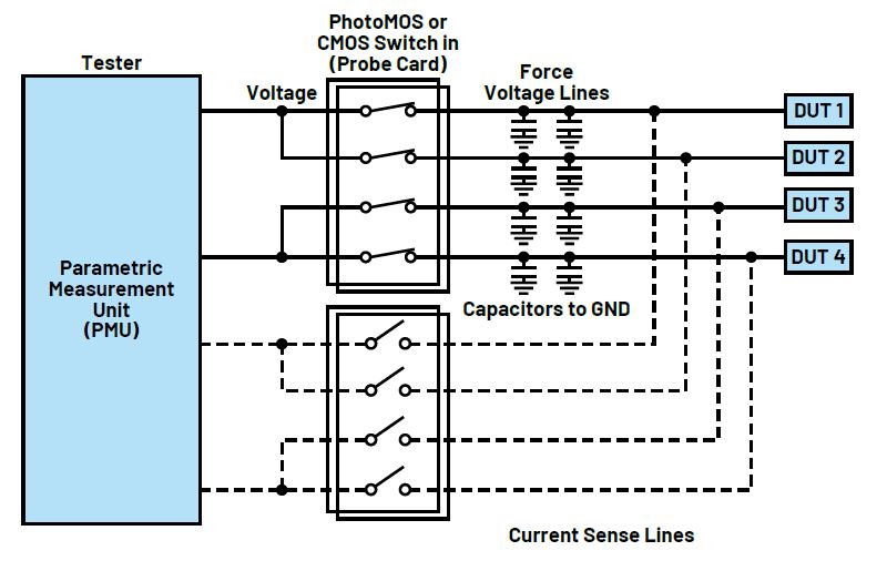
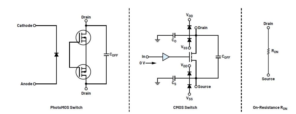
Figure 1 demonstrates how switches can facilitate the creation of a matrix configuration, enabling one PMU to evaluate multiple DUTs. This configuration enhances the flexibility and scalability of ATE systems by reducing the need for multiple PMUs and wir- ing complexity, which is crucial for high volume or multidevice testing setups.
Switch Architectures
To understand the evaluation study (that is, the comparison done between a PhotoMOS switch and a CMOS switch using developed hardware evaluation boards) and the subsequent results gath- ered, it is necessary to show benchmark comparisons between a PhotoMOS switch and a CMOS switch. The best place to start is
with the switch architectures for both.
While the architectures for a CMOS switch and PhotoMOS switch appear to be different, Figure 2 shows the off capacitance (COFF) when the switches are off. This parasitic capacitance is across the input source pin and the output pin.
For a PhotoMOS switch, the COFF is between the drain output pins. In addition, the PhotoMOS switch has input to output capaci- tance (or drain capacitance) as well as an input capacitance on the light emitting diode (LED) stage used for the turn-on and turn-off of the output MOSFETs.
For a CMOS switch, the COFF is between the source and the drain pins. In addition to the COFF, there are the drain capacitance (CD) and source capacitance (CS) to ground for a CMOS switch. These capacitances to ground are also a complaint point received from customers using CMOS switches.

When either switch is enabled to pass input signals through to the output, the on-resistance (RON) is across the source and the drain pins. By understanding these architectural details, it becomes easier to analyze performance metrics like capacitance, RON, and switching behavior in evalua- tion studies, ensuring the correct switch type is chosen for specific applications.
Switch Specifications and Value Added
A better way to qualify and quantify the switches is to look at the added value contribution in a system design application. As mentioned, for the application referenced in Figure 1, the ADG1412 is well suited for such applications and can be easily deployed in lieu of a PhotoMOS switch. This CMOS switch is a quad single-pole, single-throw (SPST) device with excellent features like power handling, response time, or on-resistance and low leakage. By comparing the CMOS switch performance across relevant metrics as illustrated in Table 1, a scorecard evaluation allows designers to quantify its merit against other alternatives. This could reveal more about the device’s efficiency in signal switching, especially in complex or sensitive electronic systems.

Off-Isolation: Capacitance When Switch Is Off
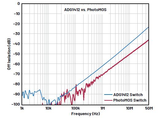
The off-isolation plots (Figure 3) for both switches indicate a high suppression (–80 dB at 100 kHz) of input signals not reaching the output. PhotoMOS performs marginally better with -10 dB as frequency increases. For the switching application shown in Figure 1, which indicates direct current (DC) switching, the switch capacitances do not matter—rather the switch benchmark parameters of interest are low leakage current, fast turn-on speeds, and insertion loss.
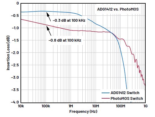
Insertion Loss: Switch On-Resistance
A switch with low RON is critical. The I*R (voltage) drop limits the system performance. Low RON variation from part to part and over temperature reduces measurement error. The insertion loss plot in Figure 4 shows the PhotoMOS switch tailoring down –0.8 dB at 100 kHz compared to the CMOS switch (–0.3 dB) at the same frequency. This reinforces the low RON (1.5 Ω) for the CMOS switch.

Switch Turn-On Time
From the onset of a drive enable/logic voltage applied to either switch that causes the switch to close and pass input signals to output, expect a significant delay time for the case of using a PhotoMOS switch (Figure 5). This slow turn-on speed is due to the input capacitance on the LED input stage and the delay due to internal circuitry used for energy conversion from current to voltage required to drive the gates of the MOSFETs. These slow turn-on speeds have been a notable point of dissatisfaction among customers and one that slows and impacts the overall system application. The CMOS switch has a fast turn-on speed (100 ns) desired in system applications over a PhotoMOS switch (200,000 ns). This represents a reduced magnitude of two thou- sand times (×2000).
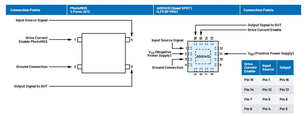
Design-Migration: PhotoMOS to ADG1412 Switch
For systems using PhotoMOS switches where issues exist in terms of measurement inaccuracies, system hogging due to slow turn-on speeds, and the inability to create channel density, upgrading to new development with the CMOS switch is amazingly easy. Figure 6 shows the points of connections for a PhotoMOS switch mapped to that of the CMOS switch. Therefore, system designs can use available switches to increase channel density at a reduced cost.
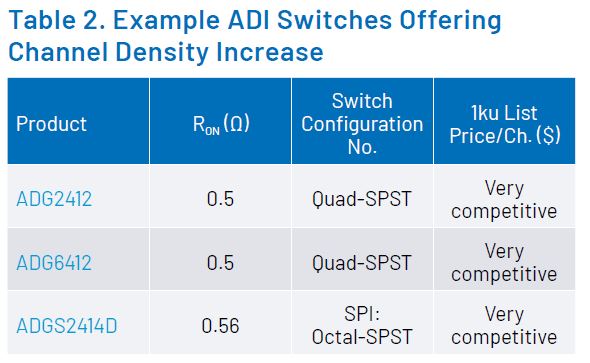
ADI Switches Offering Channel Density Increase
Table 2 lists examples of some ADI switches offering channel density increase. The switches have performance advantages like those of the ADG1412, possess a much lower on-resistance of at least 0.5 Ω, and come with a reduction in cost compared to PhotoMOS switches. These switches are available in both serial peripheral interface (SPI) and parallel interface enabling simple connections to control processors.
Table 2. Example ADI Switches Offering Channel Density Increase
Conclusion
This analysis highlights the potential of using a CMOS switch. The ADG1412 is a suitable alternative to a PhotoMOS switch in ATE applications. The benchmark comparison shows that the CMOS switch meets or exceeds performance expectations, especially in scenarios where switch capacitance or drain capacitance is not critical. Moreover, the CMOS switch offers notable advantages, including higher channel density and cost-effectiveness.
ADI’s CMOS switch portfolio, which includes options with lower on-resistance and both parallel and SPI control interfaces, fur- ther enhances the case for their adoption in ATE systems.
Please visit the following links below for more information on the switches on offer.
Selection Table for Analog Switches Multiplexers Switches and Multiplexers—Cheat Sheet Document
About the Author
Edwin Omoruyi is a senior product applications engineer in the Instrumentation Business Unit at Analog Devices, Ireland. He graduated from the Limerick Institute of Technology in 2007 with a B.Eng. honors degree in electronics systems engineering, and from the University of Limerick in 2010 with an M.Eng. honors degree in very large-scale integration (VLSI). Edwin rejoined ADI in 2023 after he previously worked in the Automotive and Cabin Electronics Business Unit as an applications engineer from 2010 to 2018. Outside of ADI, he worked as a system architect on AD/ADAS sensing applications in the automotive industry and manufacturing sector