
MOSFET technologies are excellent switches in a wide range of applications with varying requirements, including power management circuits and motor drives. The commercial introduction of vertical diffused MOSFET structures with a lateral channel offered an appealing alternative to bipolar technologies [1]. But the high on-state resistance limited the current-handling capabilities of these devices, and hence their use in power electronic applications.
The appearance of the first trench gate MOSFETs marked a milestone for the broad adoption of field-effect transistors in power electronics [2]. Moving the channel vertically, the device virtually removed the JFET region and reduced the on-state resistance. Advancements in manufacturing technology increased the cell density and with it, the channel width, offering progressively lower on-state resistances. However, this cell density increase also brought significant disadvantages. The gate-drain and gate-source capacitance both increase linearly with the number of trenches, i.e., with the cell density.

A MOSFET is uniquely controlled through its gate terminal, so the gate driver circuitry must provide the total gate charge (QG) required to turn on the transistor. In the case of high switching frequency applications like SMPS, the lowest gate charge is desirable to proportionally reduce driving losses. Larger gate-drain charge (QGD) values impact the transient speed, resulting in increased switching losses, forcing longer dead-times.

The introduction of charge-compensated structures, exploiting the same principle as super junction devices, marked the beginning of a new era. The first of these devices used an insulated deep field-plate as an extension of the gate to enable the lateral depletion of the drift region in the off state. This achieved a substantial reduction in the on-state resistance [3]. It was only by isolating the field plate from the gate and connecting it to the source that devices with improved gate and gate-drain charges were created [4]. When introduced, these devices showed best-in-class performance with the following features, eventually becoming an industry standard:
- Low gate charge and gate-drain charge characteristics
- High switching speeds
- Good avalanche ruggedness
New MOSFET devices should improve all figures of merit, as losses are associated with both charges (switching) and on-state resistance (conduction). A novel cell-design that explores a true three-dimensional charge compensation meets these requirements [5].
State-of-the-art power MOSFET technologies commonly use an insulated deep field-plate, separated from the gate electrode above, combined with a stripe layout (figure 1, left). The new approach separates the field-plate trench (now forming a needle-like structure) from the gate (now forming a grid surrounding the needles, figure 1, right). This increases the silicon area for current conduction and reduces the overall on-state resistance.
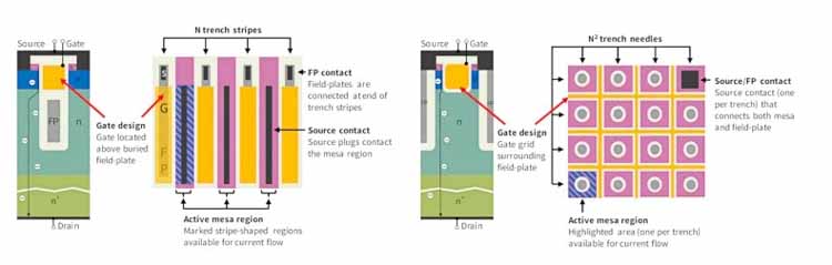
To further reduce the FOMG = RDS(on) × QG and FOMGD = RDS(on) × QGD values, the gate trench is completely redesigned, minimizing its lateral extension. However, the reduced dimensions of the gate impose a challenge because using polysilicon as the gate material results in unacceptably large internal gate resistances. The standard approach to address this problem is to introduce gate fingers to shorten the gate element lengths, thus reducing the overall distributed gate resistance.
Unfortunately, these finger structures consume space at the cost of the active area available for current conduction. Introducing gate fingers will therefore reduce the internal gate resistance, but increase the on-state resistance of the chip. To avoid this area wastage, a metal gate system is introduced to reduce the internal gate resistance and significantly improve the gate resistance uniformity over the chip.
Together with the direct connection of the field plates to the source metal, a new device setup is realized. This setup ensures a fast and homogeneous transition at turn-on and turn-off, minimizing switching losses and reducing the risk of an unwanted (dV/dt)-induced parasitic turn-on of the MOSFET. The direct connection of the field plates also practically eliminates any resistance in series with the output capacitance, minimizing the conduction losses during charging and discharging.
Figure 2 summarizes the impressive device parameter improvements for various voltage classes in all relevant parameters over the predecessor technology. Thanks to the new advanced cell design, the device on-state resistance is dramatically reduced, allowing a much higher current in the same package footprint. The innovative gate-trench engineering of the new device also greatly improves both gate- and gate-drain specific capacitances, reflected in the respective figures-of-merit: FOMG and FOMGD.
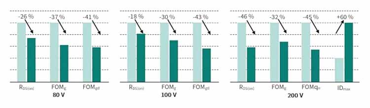
FOMG reduction helps achieve better efficiencies, especially at light load conditions because of reduced driving losses. This is particularly important for an SMPS operated at high switching frequencies and in applications like motor drives with a large number of paralleled MOSFETs. Here, the low gate charge also relaxes the requirements on the gate driver’s current capability. Additionally, the low QGD enables fast switching transients, lowering switching losses.
In case of the new 200 V technology, it is additionally important to reduce the reverse recovery charge with respect to the predecessor technology generation. This is important for:
- Lowering the switching losses
- Improving the EMI behavior
- Ensuring a high commutation ruggedness
DC-DC converters are extensively utilized in telecom and datacom power systems, commonly as isolated DC-DC intermediate bus converters (IBC) in the overall conversion chain from a nominal 48 V input. These converters step down the line voltage to an intermediate voltage, such as 12 V, to feed the downstream point-of-load (PoL) converters. Because of continuous improvements in MOSFET technology, power density has increased enough for a regulated IBC in a standard quarter-brick form factor to deliver up to 1 kW of power continuously.
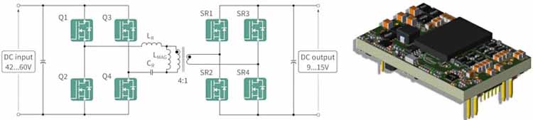
In modern datacenters, the nominal 48 V distribution bus ranges between 40 V and 60 V. The resonant LLC topology (figure 3, left) is a popular choice for IBCs, enabling high-efficiency conversion with high power density [6]. Operating with a fixed switching frequency, the LLC IBC behaves like a DC transformer (DCX) realizing a fixed-ratio down conversion (e.g., 4:1). The LLC DCX converter attains zero-voltage switching (ZVS) in the primary-side switches Q1 to Q4 regardless of the output load level.
ZVS is achieved through the transformer magnetizing inductance LMAG. Its value is defined accounting for the MOSFETs’ output capacitance COSS, as the magnetizing current ILMAG must fully charge and fully discharge COSS during the dead-time. This condition must be fulfilled over the entire input voltage range, ensuring all primary-side MOSFETs operate in soft switching. Each MOSFET in the full bridge is switched at a constant 50 percent (minus the dead-time) duty cycle ratio.
The inductor LR forms a series-resonant circuit with the resonant capacitor CR, building up a quasi-sinusoidal current fed through the transformer to the secondary side, rectified by the synchronous rectification stages SR1 to SR4. The SR MOSFETs operate in ZVS and zero-current switching (ZCS), virtually eliminating most losses associated with their commutation.
Figure 3 (right) shows the employed 1 kW test board with a standard quarter-brick form factor with the parameters detailed in table 1.
| Parameter | Value |
| Transformer turns ratio | 4:1 |
| LLC converter resonant frequency | 310 kHz |
| Primary-side full-bridge MOSFETs | ISC014N08NM6, 80 V, PQFN 5 mm × 6 mm, RDS(on),max = 1.45 mΩ |
| Secondary-side full-bridge MOSFETs | IQE006NE2LM5, 25 V, PQFN 3.3 mm × 3.3 mm Source-Down, RDS(on),max = 0.65 mΩ, two-paralleled |
The significantly improved device parameters allow the replacement of two paralleled OptiMOS™ 5 BSC030N08NS5 power MOSFETs in each position of the primary full bridge with one OptiMOS 6 ISC014N08NM6 power MOSFET. Figure 4 compares the efficiency and device temperatures. With the new devices, the overall efficiency improves over the full output current range, with a peak improvement of almost 0.8 percent at low load. Despite using one device instead of two, the package temperature also decreases.
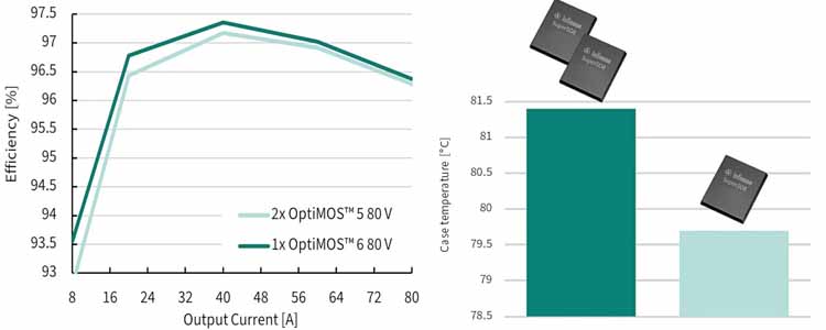
This efficiency improvement comes from the lower gate and gate-drain charges and the practically eliminated internal series resistance to the output capacitance. The LLC avoids losses because of the stored charge in the output capacitance of the MOSFET because this charge swings from one MOSFET to the other instead of being dissipated during a hard turn-on of the device. However, this swing current causes conduction losses because of PCB tracks, transformer windings, and the internal equivalent series resistance connected to the MOSFET output capacitance, the latter being massively reduced with the new devices.
Inverting buck-boost DC-DC converters in -48 V telecom power systems are used in the supply of the RF power amplifiers (RFPAs), which need supply voltages ranging from +28 V (for use in LDMOS RFPAs) up to +50 V (for use in GaN RFPAs).
The investigated evaluation board provides an output voltage of 12 V, suitable for telecom equipment except for RFPAs and those which do not require functional/safety isolation. This configuration requires MOSFETs with a blocking voltage of 100 V, making it an excellent means to study the performance of the new OptiMOS 6 100 V MOSFET in a soft-switching topology. The board, based on an interleaved (two-phase) inverting buck-boost, delivers up to 600 W from an input voltage range of -36 V to -60 V. Figure 5 shows the basic schematic and the resulting board.
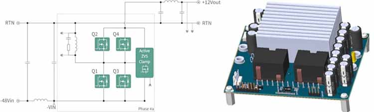
The design uses a novel active clamp auxiliary circuitry that transfers the reverse recovery charge QRR from the synchronous rectifier MOSFETs Q2 and Q4 towards the output in a non-dissipative way. This achieves ZVS turn-on for the control switches Q1 and Q3. The active clamp circuit drives down the overall switching losses in the unit, enabling the use of best-in-class devices with the lowest on-state resistance, and supporting a dramatic increase in power density [7].
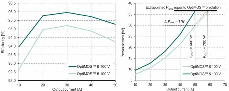
Figure 6 compares the measured efficiencies between the predecessor OptiMOS 5 BSC027N10NS5 and the new OptiMOS 6 100 V ISC022N10NM6 MOSFETs. The results clearly illustrate the huge impact of this advanced technology with an impressive efficiency gain of up to 1 percent. The higher efficiency goes hand-in-hand with the lower losses of 7 W, indicating a power density increase of 15 percent. This loss reduction is due to the lower on-state resistance, lower gate charge, and lower reverse-recovery charge being transferred to the output by the active ZVS clamp circuit.
The performance of the latest OptiMOS 6 200 V technology under hard-switching conditions is investigated in a motor drive application. The modified, commercially available inverter – sized to drive a 65 kW AC induction motor – employs a common B6 topology with a nominal input voltage of 144 V, an average current output of 135 Arms, and a 1-minute phase RMS output current of 500 Arms.
The power board contains 96 MOSFETs overall in the standard TO-263-3 (D2PAK) package with 16 devices paralleled in each leg, using an insulated metal substrate power base for superior heat transfer with increased reliability and performance.
| Family | Device | On-state resistance |
| OptiMOS™ 6 | IPB068N20NM6 | 6.8 mΩ |
| OptiMOS™ 3 | IPB117N20NFD | 11.7 mΩ |
| Parameter | Value |
| Switching frequency | 10 kHz |
| Dead-time | ~1 µs |
| Motor load phase current | 160 Arms |
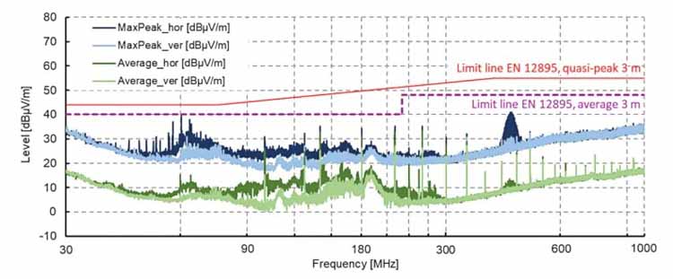
Figure 7 presents the overall mean losses per MOSFET as well as the separate conduction, turn-on, and turn-off losses. The overall loss reduction accounts for a remarkable 36 percent, with all loss contributors lowered compared with the predecessor generation. In addition, this application benefits from the much lower threshold voltage variation of the OptiMOS 6 devices because this supports a balanced current sharing. Further, this significantly improved performance does not degrade the EMI behavior, as indicated in figure 8 by the radiated emission measurement according to the applicable standard EN 12895.

This article introduces Infineon’s latest power MOSFET technology family. The new generation with the latest OptiMOS technology delivers improvements in all important device parameters and combines the benefits of low on-state resistance with a superior switching performance. The remarkable progress in the overall device performance is enabled by substantial improvements at the device technology level. This has culminated in a unique device structure, which is the first to employ three-dimensional charge compensation combined with a gate grid and the first ever use of a metal gate in a trench power MOSFET. The new design provides an unmatched homogeneity of the gate and field-plate resistance across the chip, enhancing the system efficiency in tested applications across all load conditions by:
- Reduction achieved in the on-state resistance
- Dramatically lowered total gate charge
- Low gate-drain charge together with a low output charge
- Improved switching homogeneity across the device area
References
[1] R.K. Williams, M.N. Darwish, R.A. Blanchard, R. Siemieniec, P. Rutter and Y. Kawaguchi, “The Trench Power MOSFET: Part I – History, Technology, and Prospects”, IEEE Transactions on Electron Devices, Vol. 64, No. 3, pp. 674-691, 2017
[2] H.-R. Chang, R. D. Black, V.A.K. Temple, W. Tantraporn, and B.J. Baliga, “Self-aligned UMOSFET’s with a specific on-resistance of 1 mW cm2”, IEEE Transactions on Electron Devices, Vol. ED-34, no. 11, pp. 2329–2334, 1987
[3] J. Ejury, F. Hirler and J. Larik, “New P-Channel MOSFET Achieves Conventional N-Channel MOSFET Performance”, Proc. PCIM, Nuremberg, Germany, 2001
[4] A. Schlögl, F. Hirler, J. Ropohl, U. Hiller, M. Rösch, N. Soufi-Amlashi and R. Siemieniec, “A new robust power MOSFET family in the voltage range 80 V – 150 V with superior low RDS(on), excellent switching properties and improved body diode”, Proc. EPE, Dresden, Germany, 2005
[5] R. Siemieniec, M. Hutzler, C. Braz, T. Naeve, E. Pree, H. Hofer, I. Neumann and D. Laforet, “A new power MOSFET technology achieves a further milestone in efficiency”, Proc. EPE, Hannover, Germany, 2022
[6] B. Yang, F.C. Lee, A.J. Zhang, and G. Huang: LLC resonant converter for front end DC/DC conversion, APEC 2002, Dallas, USA
[7] Infineon Technologies AG (2021, 8.), Application note: “XDPP1100 two-phase interleaved buck-boost”
Author biographies
Ralf Siemieniec is a Senior Principal Engineer working on the development of technology concepts for silicon and silicon carbide MOSFET. He received his engineering and doctor’s degree in electrical engineering from the Technical University of Ilmenau in Germany.
Simone Mazzer is a System Engineer at Infineon Technologies, focusing on high-density DC-DC converters and VRMs for datacenters. He received his M.Sc. degree in electronic engineering from the University of Udine in Italy in 2020.
Cesar Augusto Braz is a product definition engineer of 100 V and 120 V MOSFETs. In the past, Cesar has held roles as SMPS and DC power system designer for telecom. He holds a master’s degree in electronics and computing engineering from Instituto Tecnologico de Aeronautica in São José dos Campos in Brasil. Elvir Kahrimanovic is a Principal Engineer at Infineon Technologies, focusing on medium voltage MOSFETs in various applications. He earned his master’s degree in electrical and computer engineering from the Illinois Institute of Technology (IIT) in Chicago in 2011.