

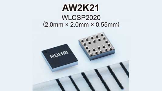
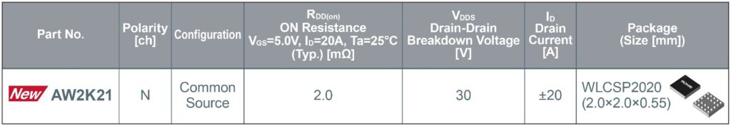
ROHM has developed a 30V N-channel MOSFET — AW2K21 — in a common-source configuration that achieves an industry-leading ON-resistance of 2.0mΩ (typ.) in a compact 2.0mm × 2.0mm package.
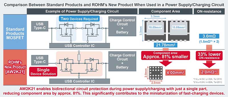
With the rise of compact devices featuring large-capacity batteries, such as smartphones, the need for fast charging functionality to shorten charging times continues to grow. These applications require bidirectional protection to prevent reverse current flow to peripheral ICs and other components when not actively supplying or receiving power. What’s more, fast charging involves high current power transfer, leading smartphone manufacturers to demand stringent specifications for MOSFETs, including a maximum current rating of 20A, breakdown voltage between 28V and 30V, and an ON-resistance of 5mΩ or less. However, meeting these requirements with standard solutions typically necessitates the use of two large low ON-resistance MOSFETs, increasing board space along with mounting complexity.
In response, ROHM developed an ultra-compact low ON-resistance MOSFET optimized for fast high-power charging. The AW2K21 adopts a proprietary structure that enhances cell density while minimizing the ON-resistance per unit chip area. Two MOSFETs are integrated into a single package, allowing a single part to support bidirectional protection applications (commonly required in power supply and charging circuits).
The proprietary structure also places the drain terminal on the top surface, unlike on the backside in standard vertical trench MOS structures. This enables the use of a WLCSP, which achieves a larger chip-to-package area ratio that further reduces ON-resistance per unit area. As a result, the new product not only minimizes power loss but also supports high current operation, making it ideal for high-power fast charging applications despite its ultra-compact size.
For example, in power supply and charging circuits for compact devices, standard solutions typically require two 3.3mm × 3.3mm MOSFETs. In contrast, the AW2K21 can achieve the same functionality with a single 2.0mm × 2.0mm unit, reducing the footprint and ON-resistance by approximately 81% and 33%, respectively. Even compared to similarly sized GaN HEMTs, ON-resistance is decreased by up to 50%, contributing to lower power consumption and increased space savings across a variety of applications.
The AW2K21 is also suitable for use as a unidirectional protection MOSFET in load switch applications, where it maintains the industry’s lowest ON-resistance. At the same time, ROHM is further pushing the limits of miniaturization with the development of an even smaller 1.2mm × 1.2mm model.
Going forward, ROHM remains dedicated to supporting the miniaturization and energy efficiency of electronic systems through compact, high-performance solutions that contribute to the realization of a sustainable society.
Key Product Characteristics
Application Examples
- Smartphones
- Tablets
- Laptops
- VR (Virtual Reality) headsets
- Wearables
- Portable gaming consoles
- Compact printers
- LCD monitors
- Drones
And other applications equipped with fast charging capability.
Online Sales Information

Sales Launch Date: April 2025
Pricing: $3.5/unit (samples, excluding tax)
Online Distributors: DigiKey™, Mouser™ and Farnell™
Applicable Part No: AW2K21
The product will be offered at other online distributors as it becomes available.
Terminology
MOSFET (Metal Oxide Semiconductor Field Effect Transistor)
A field-effect transistor (FET) featuring a metal oxide semiconductor structure (the most commonly used type). It consists of three terminals: gate, drain, and source. Applying a voltage to the gate (control terminal) regulates current flow from the drain to the source.
N-channel MOSFETs turn ON when a positive voltage is applied to the gate relative to the source. A common-source configuration MOSFET integrates two transistor elements that share a single source terminal.
ON-Resistance
The resistance between the Drain and Source of a MOSFET when it is in the ON state. A smaller RDS(on) reduces power loss during operation.
Breakdown Voltage
The maximum voltage that can be applied between the drain and source terminals of a MOSFET without causing damage. Exceeding this limit results in dielectric breakdown, potentially leading to device failure or malfunction.

WLCSP (Wafer Level Chip Scale Package)
An ultra-compact package in which terminals and wiring are formed directly on the wafer before separated into individual chips. Unlike general packages where the chips are cut from the wafer and then molded with resin to form terminals, WLCSP allows the package size to match the chip itself, making it possible to further reduce size.
GaN HEMT
GaN (Gallium Nitride) is a compound semiconductor material used in next-generation power devices. It offers superior physical properties over conventional silicon, enabling higher frequency operation with faster switching speeds. HEMT stands for High Electron Mobility Transistor.
Note: DigiKey™, Mouser™ and Farnell™ are trademarks or registered trademarks of their respective companies.