FREMONT, Calif. — Lam Research Corp. today unveiled VECTOR® TEOS 3D, a breakthrough deposition tool engineered specifically for the advanced packaging of next-generation chips required for artificial intelligence (AI) and high-performance computing (HPC) applications. TEOS 3D is purpose-built to solve critical challenges in 3D stacking and high-density heterogeneous integration. It provides ultra-thick, uniform, inter-die gapfill, leveraging a proprietary bowed wafer handling approach, innovations in dielectric deposition, and enhanced monitoring by Lam Equipment Intelligence® technology. TEOS 3D is installed at leading logic and memory fabs around the world.
“VECTOR TEOS 3D deposits the industry’s thickest, void-free, inter-die gapfill films, customized to meet the challenging requirements of advanced die stacking integration schemes, even on ultra-stressed, high-bow wafers,” said Sesha Varadarajan, senior vice president of the Global Products Group at Lam Research. “It’s another powerful addition to our best-in-class advanced packaging portfolio, which delivers the differentiated, atomic-level innovations chipmakers need to scale beyond Moore’s Law and into the AI era.”

Addresses Manufacturing Pain Points
The explosive growth of AI is driving the need for new devices that can support increasingly data-intensive workloads. Chipmakers are turning to 3D advanced packaging to integrate multiple dies into chiplet architectures to enable AI compute. By bringing memory and processing closer together to optimize electrical pathways, chiplet designs can improve processing speed, and pack more power into smaller form factors. However, as chiplets scale taller and become more complex, they present a range of new manufacturing hurdles, from stress during processing that can distort or bow a wafer’s shape, to cracks and voids in films that cause defects and lower yield.

TEOS 3D conquers a range of critical advanced packaging production challenges, excelling at handling bulky, high-bow wafers precisely and reliably. With nanoscale precision, it deposits specialized dielectric films of up to 60 microns thick between dies, with scalability to deposit films greater than 100 microns. The films provide essential structural, thermal and mechanical support to prevent common packaging failures such as delamination. TEOS 3D also features Lam’s novel clamping technology and an optimal pedestal design that provides exceptional stability when processing thick wafers, enabling uniform film deposition even when dealing with extreme wafer bow.
Other highlights include:
- The first solution for single-pass processing of crack-free films more than 30 microns thick, significantly enhancing yield and process time.
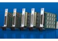
- Unique quad station module (QSM) architecture to boost productivity: Lam’s proven QSM architecture features four distinct stations to enable parallel processing and reduce bottlenecks. The modular design helps deliver nearly 70%1 faster throughput and up to 20% improvement in cost of ownership compared to Lam’s previous generation of gapfill solutions.
- Lam Equipment Intelligence® technology for process repeatability: Built into TEOS 3D, Equipment Intelligence solutions boost equipment performance and reliability, and drive yield improvement by using smart technology to monitor processes, fix issues faster, and automate routine tasks.
- Enhanced energy efficiency: Integrated high-efficiency RF generators and ECO Mode peripheral control reduce energy consumption while improving process precision.
Joins an Industry-Leading Suite of Advanced Packaging Solutions
Leveraging the company’s 15 years of leadership in advanced packaging and decades of expertise in dielectric films, TEOS 3D builds on Lam’s existing VECTOR® Core and TEOS product families, representing continuous innovation in materials and processes for integrated packaging. It is part of a comprehensive product portfolio of industry-leading solutions that addresses critical challenges and drives innovation and productivity across the advanced packaging workflow.