
Electronics Era

  • About Us
  • Advertise with Us
  • Contact Us
  • e-Mag
  • Webinars
Header logo on website
Advertisement
Advertisement
Menu
  • Home
  • News
    • Industry News
    • Product News
  • TECH ROOM
    • Sensor
    • VR / AR
    • Embedded
    • Medical Electronics
    • Industry 4.0
    • Robotic
    • Automation
    • Smart Machine
    • Component
    • MCU
    • Manufacturing
    • Aerospace & Defence
    • Security
    • Policy
    • RENEWABLES
      • Sustainability
  • Semiconductor
    • AUTOMOTIVE ELECTRONICS
      • EVs
      • HEVs
      • ADAS
      • Connected Cars
    • IoT-Internet of Things
      • Development Kit
      • IoT Design
    • Power Electronics
      • AC-DC/DC-DC Converters
      • Mosfets
      • IGBTs
      • LEDs
  • T & M
    • 5G testing
    • Oscilloscopes
    • SDN & NFV
    • RF & Wireless
  • AI/ML
  • Telecom
    • 5G/6G
  • Future Tech
    • Data Center
    • Cloud Computing
    • Big Data Analytics
  • Webinars
  • Editor’s Pick
    • Tech Article
    • Tech Blog
    • White Papers
    • EE-Tech Talk
    • Market Research
    • Videos
  • EE Awards
    • EE Awards 2025
    • EE Awards 2024
  • MORE
    • E-Mag
    • Events
    • MAGAZINE Subscription
    • Contact Us
Home TECH ROOM SMT/PCB/EMS

Fuji Succeeds in World-First 016008 mm Component Placement

Pursuing next-generation placement technology in the AI era

Nimish by Nimish
February 3, 2026
in SMT/PCB/EMS
Reading Time: 3 mins read
Fuji Corporation

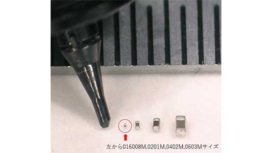
016008 mm (006003") shown beside commercially available components

Share on FacebookShare on TwitterShare on LinkedIn

Fuji Corporation (headquarters: Chiryu, Aichi; Representative Director, President and CEO: Joji Isozumi; hereinafter referred to as “Fuji”) is pleased to announce that it has achieved the world’s first placement of 016008 mm (0.16 x 0.08 mm or 006 x 003 inches) size components on printed circuit boards (PCBs) with its SMT pick and place machine, NXTR, following the successful development of machine technology designed to handle next-generation ultra-small electronic components. This achievement was showcased at the 40th NEPCON JAPAN – Electronics R&D and Manufacturing Technology Expo exhibition on January 21, 2026 at Tokyo Big Sight.

Note: Based on Fuji’s research (as of January 15, 2026).

There is currently an accelerating shift toward edge AI, where AI processing is performed on the device itself. An era is also emerging in which a wide range of everyday devices, including smartphones, wearable devices, and even medical and healthcare equipment, are autonomously analyze information. Amid these trends toward greater functionality in electronic devices, the number of mounted electronic components is increasing significantly. As a result, further miniaturization and higher-density integration of electronic components have become critical and unavoidable technological challenges.

Even the 0201 mm (0.25 x 0.125 mm, 008004 inches) size component, which has long been considered the smallest standard among currently commercialized electronic components, will eventually reach its limits in the pursuit of higher density to integrate more electronic functions into limited board space. A next-generation component size, 016008 mm (006003″), is being developed in response. 016008 mm (006003″) size components require approximately half of the placement area compared to 0201 mm size components, allowing for higher-density circuit designs.

Four key control technologies enabling the world’s first 016008 mm (006003″) size component placement
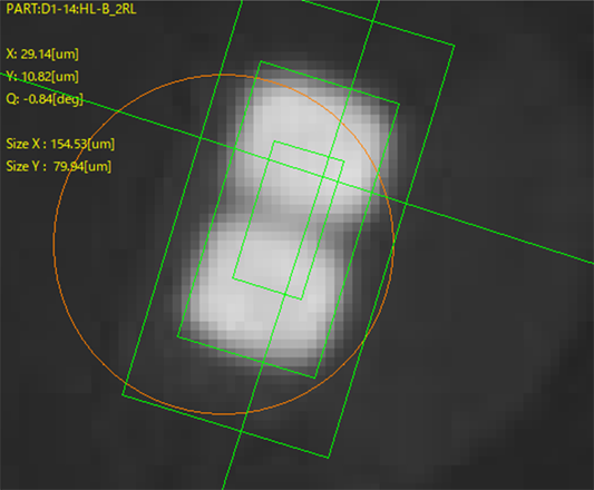
016008 mm (006003″) size components
captured by a high-resolution camera

Fuji has been providing high-speed, high-accuracy pick and place machines capable of reliably handling very small components. Advancements in the following four key control technologies have made the world’s first placement of 016008 mm (006003″) size components on PCBs possible.

1. Stance recognition during handling

The orientation and stance of very small components are checked in real time to ensure optimal part handling.

2. Highly-accurate part pickup control

Deviations in pickup position and the effects of static electricity are addressed for stable part pickup.

3. Super-fine control of placement pressure

Pressure is precisely controlled to ensure that very small components are not damaged during placement.

4. Ultra-high precision placement positioning control

With nano-level position compensation, the highest level of placement accuracy in the industry is achieved.

Aiming to build a comprehensive solution for next-generation very small component placement

To place components 016008 mm (006003″) or smaller, it is essential to optimize not only the placement process but also all processes related to placement, including panel design, solder paste materials, stencils, reflow, and inspection, at a high level. Fuji is developing machine technology for placement robots while deepening cooperation with partners to build a total process solution, including production materials and related materials, taking the race for the miniaturization of electronic components to a


Tags: Component PlacementFuji Corporation
Nimish

Nimish


Join Our Newsletter

* indicates required
Electronics Era

Electronics Era, India's no.1 growing B2B news forum on Electronics and Cutting Edge Technology is exploring the editorial opportunity for organizations working in the Electronics Manufacturing Services(EMS) Industry.

Follow Us

Browse by Category

  • 5G testing
  • 5G/6G
  • AC-DC/DC-DC Converters
  • ADAS
  • Aerospace & Defence
  • AI/ML
  • Automation
  • AUTOMOTIVE ELECTRONICS
  • Big Data Analytics
  • Blockchain
  • Cloud Computing
  • Component
  • Connected Cars
  • Data Center
  • Editor's Desk
  • EE-Tech Talk
  • Electronics Components
  • Embedded
  • EVs
  • Future Tech
  • HEVs
  • Industry 4.0
  • Industry News
  • IoT Design
  • IoT-Internet of Things
  • LED & Lighting
  • LEDs
  • Manufacturing
  • Market Research
  • MCU
  • Medical Electronics
  • Mosfets
  • News
  • Oscilloscopes
  • Policy
  • Power Electronics
  • Product News
  • RENEWABLES
  • RF & Wireless
  • Robotic
  • SDN & NFV
  • Security
  • Semiconductor
  • Sensor
  • Smart Machine
  • SMT/PCB/EMS
  • Sustainability
  • T & M
  • Tech Article
  • Tech Blog
  • TECH ROOM
  • Telecom
  • Uncategorized
  • VR / AR
  • White Papers

Recent News

Keysight Technologies

Keysight Addresses Cross-Domain Physics Issues That Leave Electronic Designs Vulnerable to Late-Stage Failure

July 22, 2026
ROHM

ROHM has Developed a New Evaluation Board, the BD83070GWL-EVK-002

July 22, 2026
  • About Us
  • Advertise with Us
  • Contact Us

© 2022-23 TechZone Print Media | All Rights Reserved

No Result
View All Result
  • Home
  • News
    • Industry News
    • Product News
  • TECH ROOM
    • Sensor
    • VR / AR
    • Embedded
    • Medical Electronics
    • Industry 4.0
    • Robotic
    • Automation
    • Smart Machine
    • Component
    • MCU
    • Manufacturing
    • Aerospace & Defence
    • Security
    • Policy
    • RENEWABLES
      • Sustainability
  • Semiconductor
    • AUTOMOTIVE ELECTRONICS
      • EVs
      • HEVs
      • ADAS
      • Connected Cars
    • IoT-Internet of Things
      • Development Kit
      • IoT Design
    • Power Electronics
      • AC-DC/DC-DC Converters
      • Mosfets
      • IGBTs
      • LEDs
  • T & M
    • 5G testing
    • Oscilloscopes
    • SDN & NFV
    • RF & Wireless
  • AI/ML
  • Telecom
    • 5G/6G
  • Future Tech
    • Data Center
    • Cloud Computing
    • Big Data Analytics
  • Webinars
  • Editor’s Pick
    • Tech Article
    • Tech Blog
    • White Papers
    • EE-Tech Talk
    • Market Research
    • Videos
  • EE Awards
    • EE Awards 2025
    • EE Awards 2024
  • MORE
    • E-Mag
    • Events
    • MAGAZINE Subscription
    • Contact Us

© 2022-23 TechZone Print Media | All Rights Reserved

Advertisement
Advertisement