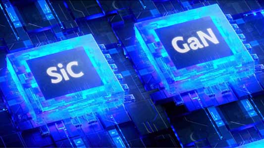
Power electronics is in the middle of a materials-driven inflection point. After decades of silicon MOSFET and IGBT optimization, wide-bandgap (WBG) semiconductors—chiefly Gallium Nitride (GaN) and Silicon Carbide (SiC)—are now enabling step changes in efficiency, switching frequency, and power density. In practical terms, that translates to smaller chargers, lighter converters, higher-temperature operation, and reduced cooling and magnetics, with ripple effects across product industrial design, compliance, cost, and reliability engineering.
Yet GaN and SiC are not interchangeable “next-gen silicon.” Their strengths diverge sharply: GaN is a switching-speed and power-density disruptor in the sub kilovolt range, while SiC is the high-voltage, high-temperature workhorse that is reshaping traction, grid, and high-power industrial conversion. Understanding where each wins—and what new design rules come with them—has become essential for engineers building everything from USB C PD adapters to megawatt-class converters.

1. The Case for Wide-Bandgap Power Electronics
What Is a Wide-Bandgap Semiconductor?
A bandgap is the energy difference between the valence and conduction bands in a semiconductor. Traditional silicon (Si) has a bandgap of 1.12 eV, whereas GaN (~3.4 eV) and SiC (~3.3 eV) are considered wide-bandgap materials.
The wider bandgap enables:
- Higher breakdown voltages, allowing devices to operate at higher electric fields without failure.
- Lower conduction losses, improving efficiency.
- Faster switching capabilities, enabling higher frequency operation.
- Greater thermal resilience, permitting operation at elevated temperatures.
These characteristics deliver a “power performance leap,” reducing energy losses and enabling smaller, lighter, and more efficient power systems.

Why WBG Matters Today
A semiconductor’s bandgap is the energy required to free electrons for conduction. WBG materials have much larger bandgaps than silicon, enabling higher breakdown fields, higher-temperature capability, and higher-voltage operation with thinner drift regions—key ingredients for lower conduction losses at high voltage and faster switching. Source
A useful way to see “why WBG now” is to map the system-level bottlenecks that silicon has been fighting for years: switching losses that cap frequency (and keep magnetics large), thermal limits that force bigger heatsinks, and efficiency mandates (80 PLUS, data-center specs, energy regulations) that are increasingly hard to hit with legacy devices. WBG does not merely improve these constraints; it changes the feasible design space.
2. GaN vs. SiC: Material and Device Perspectives
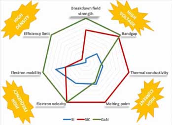
Designers often hear “GaN is faster, SiC is higher voltage,” but the why is grounded in measurable properties. PowerAmerica’s widely referenced comparison shows the scale of the jump from silicon: SiC and GaN have ~3× the bandgap of silicon and an order-of-magnitude stronger breakdown field, enabling higher-voltage devices with better loss tradeoffs.
Material snapshot (indicative values)
Si bandgap: 1.12 eV
4H‑SiC bandgap: 3.26 eV
GaN bandgap: ~3.43 eV
Breakdown field: ~300 kV/cm (Si) vs ~2200 kV/cm (4H‑SiC) vs ~3300 kV/cm (GaN)
Thermal conductivity: ~1.5 W/cm•K (Si) vs ~3.8 W/cm•K (4H‑SiC) vs ~1.3 W/cm•K (GaN)
Two immediate takeaways emerge:
SiC’s thermal conductivity advantage is real and system-relevant in high-power hardware.
GaN’s breakdown field and switching capability are outstanding, but thermal handling is more nuanced —packaging and layout become decisive.
The University of Tennessee/Oak Ridge work (a foundational reference in WBG education) also underscores that higher breakdown field reduces drift-region thickness and specific on-resistance at higher voltages; explaining why SiC and GaN can outperform silicon dramatically as voltage ratings rise.
3. Device reality: where GaN and SiC sit on the voltage–power map
In product terms, SiC devices commonly target 1200 V-class needs, high currents, and harsh thermal environments—think traction inverters and three-phase grid conversion. GaN is typically deployed as ~600–650 V-class devices in compact, high-frequency converters from consumer adapters up through server, telecom, and many industrial supplies under ~10 kW (with overlap zones). Source
TI’s application note frames it cleanly: SiC fits the high-voltage/high-power end (e.g., traction inverters, high-power solar, large grid converters), while GaN is compelling in consumer/server/telecom/ industrial power supplies and motor drives where switching speed and density dominate, and voltage ratings align.
4. Consumer Applications: GaN’s “small charger” story is really a switching-frequency story
4.1 USB‑C PD adapters and compact AC/DC supplies
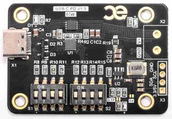
GaN’s breakout consumer win is the high-power-density USB‑C charger. However, the physics behind the shrink is not marketing magic—it is frequency. Faster switching reduces switching energy and supports operation at hundreds of kHz to MHz-class regimes, which in turn allows smaller magnetics and less bulk. TI notes GaN can enable switching frequencies over 500 kHz, yielding up to ~60% smaller magnetics in some designs.
Where silicon designs often settle into frequency/EMI/efficiency compromises, GaN expands the feasible range—especially in topologies like totem pole PFC in higher-power adapters and compact supplies. The TI comparison highlights GaN’s advantage in totem-pole PFC: zero reverse recovery (no body diode in the lateral GaN structure) and lower switching energy than SiC in that role, contributing to higher efficiency and higher switching-frequency potential.
A practical engineering narrative is captured in an EEPower technical article describing GaN-based PFC stages: GaN switching transitions can be single‑digit nanoseconds, dramatically reducing switching losses and enabling higher-frequency operation—while also raising EMI/layout stakes (more on that later).
4.2 Why totem‑pole PFC matters even in “consumer”
As power, PFC and magnetics frequently dominate levels rise (gaming laptops, monitors, compact desktops, high-wattage multi-port chargers), front-end efficiency and size. Totem‑pole PFC reduces rectifier conduction loss and can take advantage of GaN’s switching traits. TI explicitly contrasts dual-boost PFC and totem‑pole PFC, describing how WBG devices enable density and efficiency beyond what last-gen silicon/SJ MOSFET approaches could sustain.
4.3 The hidden consumer constraint: thermal comfort + enclosure limits
In consumer adapters, a few watts of loss is the difference between “cool to touch” and “unacceptable.” GaN’s ability to reduce switching and dead-time losses can lower heat generation, reducing the need for bulky thermal solutions—one-reason compact GaN chargers can deliver high wattage in palm-sized volumes. TI positions GaN as a lever for system-level thermal simplification by cutting losses and shrinking magnetics.
4.4 Wireless Charging and IoT Devices

Emerging wireless charging standards and IoT edge devices benefit from high-frequency GaN designs that support:
- High coupling efficiencies
- Compact coil drivers
- Longer operating lifetimes in thermally constrained enclosures
5. Industrial and infrastructure: SiC’s high-voltage, high-efficiency pull
If GaN’s consumer narrative is “shrink the box,” SiC’s industrial narrative is “raise the bus voltage, raise efficiency, simplify thermal management, and hit new power-density targets.”
5.1 Data centers: efficiency targets force a materials upgrade
Data centers increasingly operate under efficiency specifications that are extremely aggressive at both high and partial loads. onsemi notes AI data center PSUs may be expected to meet specifications calling for >97.5% peak efficiency across a wide load window, pushing PFC and DC/DC stages toward WBG devices.
In the PFC stage—often totem-pole PFC in multi‑kW PSUs—SiC MOSFETs are used where switching losses dominate, particularly at light loads where output-capacitance energy (EOSS) and charge metrics matter. onsemi highlights lower EOSS and gate charge as key contributors to improved efficiency and reduced switching losses.

5.2 Data-center cooling drives: SiC doesn’t just save watts—it shrinks heatsinks
Wolfspeed provides a concrete industrial example in cooling-system motor drives. In an 11 kW three-phase cooling system, replacing IGBTs with 1200 V SiC MOSFETs can yield measurable efficiency improvements, and the article emphasizes reduced switching losses (including elimination of IGBT tail current) enabling higher switching frequencies and smaller magnetics. Source
More strikingly, Wolfspeed reports system-level impacts such as substantial heatsink reduction alongside efficiency gains—an industrial designer’s dream because it reduces weight, cost, and enclosure volume while improving reliability margins.
5.3 Motor drives and factory automation: efficiency + robustness + integration
Motor drives are a massive energy lever in industry. Microchip’s industrial motor-drive discussion frames SiC’s value around higher bandgap (voltage and temperature capability), improved thermal behavior, and faster switching enabling smaller inverters and reduced cooling needs—particularly relevant as factories move toward more compact, integrated drive architectures.

5.4 Renewable Energy and Grid Systems
Solar inverters and wind turbine converters benefit from SiC at medium to high power levels:
- Higher blocking voltages and robust thermal performance
- Lower system losses improve yield and uptime
SiC devices improve:
PV string inverter efficiency
- Centralized inverter reliability
- Reduced cooling plant size
Similarly, industrial UPS systems, frequency converters, and motor drives leverage WBG technology to improve power density, reliability, and lifecycle cost.
5.5 Industrial Motors and Drives
Variable frequency drives (VFDs) control large motors in factories and process plants. Using SiC:
- Reduces switching losses
- Improves harmonic performance
- Enables higher switching frequencies
This yields:
- Reduced motor heating
- Improved torque control
- Smaller filters and reactors
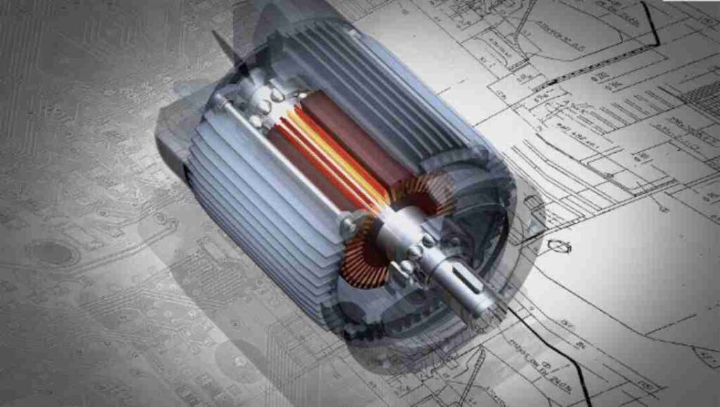
6. EV traction inverters: “industrial-grade” high-voltage switching in mass production
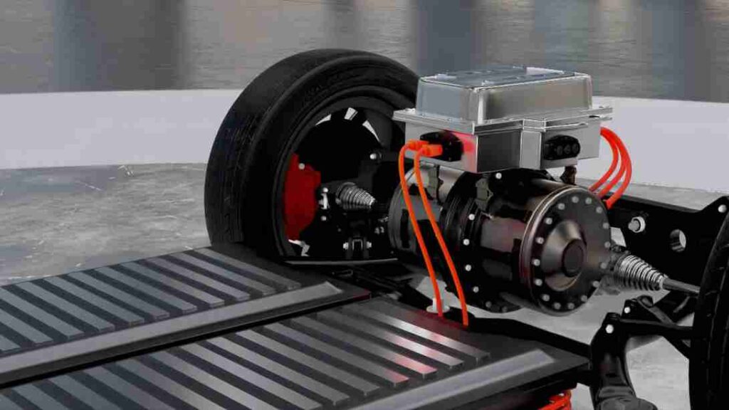
While automotive is its own vertical, EV inverters have become the flagship proof that WBG can scale. EE Times/EE Asia coverage highlights SiC’s momentum in 800 V-class traction inverters, describing how higher voltage systems stress silicon devices and how SiC enables higher efficiency, higher temperature operation, and improved packaging/integration outcomes.
A key engineering point: as platforms move from 400 V to 800 V, designers seek devices that can switch efficiently at higher voltage and temperature. The article describes SiC MOSFETs as increasingly replacing silicon IGBTs due to switching-loss reductions and thermal benefits, enabling smaller/lighter inverter implementations.
7. The design tradeoffs WBG brings: gate drive, EMI, insulation, reliability
WBG adoption is not a drop-in MOSFET swap. It is a system redesign problem, often centered on parasitic, dv/dt, di/dt, and insulation integrity.
7.1 EMI and “parasitics become first-order”
As switching speeds climb, even small inductances produce large transient voltages. RECOM’s gate-driver insulation guide gives a vivid numerical example: at 10 A/ns and 15 nH, the induced voltage can be ~150 V (V = L•di/dt), enough to disturb gate drive behavior and potentially cause spurious turn-on or shoot-through.
This reality drives the modern WBG layout playbook: Kelvin source connections where possible, minimized loop inductances, and careful partitioning between power and gate-drive return paths. The same RECOM article also explains how high dv/dt can inject displacement current through isolation capacitance (I = C•dv/dt), stressing isolation components and threatening control stability.
7.2 Reliability is no longer “HTRB/HTGB and done”—switching stress matters
TI’s reliability-focused paper argues that traditional qualification stress tests (static bias tests) do not necessarily represent real switching conditions, especially for power conversion. It proposes hard-switching stress qualification (often using double-pulse-derived methods) as an application-relevant way to validate GaN device robustness and monitor dynamic on-resistance behavior under realistic stress.
The big message for engineering teams: WBG reliability confidence is built at the intersection of device physics + packaging + switching waveform control, not from silicon-era assumptions alone.
7.3 The “efficiency paradox”: higher frequency can reduce size but increase compliance complexity
The EEPower GaN PFC discussion documents the double-edged sword: very fast switching enables high efficiency and smaller inductors, but can create hard-to-filter high-frequency disturbances if dead-time behavior and reverse conduction are not controlled. The article even notes cases where external diodes were used to tame dead-time oscillations in a specific implementation—illustrating how real-world GaN designs often involve nuanced waveform management beyond the schematic.
8. Selection guide: when to choose GaN, when to choose SiC
Choose GaN when:
- Bus voltages align with ~600–650 V-class devices (or multilevel stacking is viable).
- You are size- and weight-constrained (consumer adapters, compact server/telecom supplies).
- High switching frequency is a primary lever for shrinking magnetics and improving transient response.
Choose SiC when:
- You need 1200 V-class (and beyond) devices and high-current capability.
- Thermal headroom, harsh environments, and high bus voltages dominate the requirements.
- You want to replace IGBTs in industrial drives, grid conversion, high-power inverters, and many data-center high-power stages.
Overlap zone (<~10 kW):
This is where topology choice (totem-pole PFC, resonant DC/DC, multilevel converters), EMI limits, BOM cost, packaging availability, and supply chain often decide more than the datasheet headline specs. TI explicitly notes overlap below ~10 kW where both technologies can compete depending on topology and requirements.
9. Sustainability and Energy Impact
Wide-bandgap power electronics contribute directly to global sustainability goals by:
- Reducing energy waste in power conversion
- Lowering carbon emissions in industrial and consumer power systems
- Enabling high-efficiency electrification in transportation and renewables
For example, millions of GaN chargers replacing silicon units can save gigawatt-hours of electricity annually due to efficiency gains and lower standby losses.
In industrial settings, SiC based inverters in solar farms can increase yield and reduce maintenance costs, accelerating the adoption of clean energy.
Conclusion
GaN and SiC are no longer “future tech.” They are already changing how consumer power bricks are sized, how data centers chase efficiency at scale, and how industrial drives and high-voltage inverters hit performance targets that silicon-era solutions struggle to reach. The next wave of differentiation will come from teams that treat WBG as an end-to-end architecture choice—devices, drivers, magnetics, packaging, EMI control, insulation strategy, and reliability qualification—rather than a transistor selection exercise.