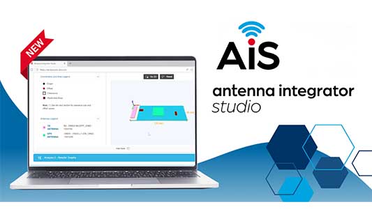

FOUNTAIN INN, S.C. – KYOCERA AVX, a leading global manufacturer of advanced electronic components engineered to accelerate technological innovation and build a better future, released a new web-based RF engineering tool — the Antenna Integrator Studio.
Wireless connectivity has become a ubiquitous capability for electronic products extending throughout every industry. As such, RF engineering has become an essential element of most electronic product designs. Selecting the right antenna and the right PCB positioning for that antenna is a crucial part of this process, as the wrong selections can result in signal attenuation, severe impedance mismatch, drastically reduced range, and excessive battery drain. Avoiding these outcomes is especially imperative in industries with strict performance, space, and environmental constraints, including the consumer electronics, automotive, medical, IIoT, telecommunications, and high-speed networking industries.

The new KYOCERA AVX Antenna Integrator Studio is designed to streamline, accelerate, and optimize the antenna selection and placement processes for RF engineers and, in turn, improve product quality, performance, and go-to-market timelines for manufacturers.
It’s also designed for easy, intuitive use. You simply enter your PCB size and the number of antennas you need, select your target frequency bands, choose your optimization priority — maximizing efficiency or minimizing cost, and click “Analyze” to instantly reveal the most suitable antennas in the most optimal positions for your PCB layout, along with interactive performance charts. You can then analyze the results in detail — evaluating efficiency, return loss, peak gain, and radiation patterns across frequency bands — and download DXF and 3D files for seamless integration into your PCB design. The Antenna Integrator Studio also makes it easy to order samples and begin prototyping and includes a roughly four-minute video tutorial that walks users through a workflow to further enhance ease of use.