

MUNICH – CEA-Leti has launched SubFAB Labs, a joint program with International SubFAB Research Labs (ISRL) that gives the semiconductor industry a pre-industrial environment to test, validate and qualify technologies that reduce the environmental impact of chip manufacturing. CEA-Leti CEO Sébastien Dauvé will announce the program at SEMICON Europa 2026.
The program’s first phase, under way at CEA-Leti’s Grenoble site, will identify and classify the gaseous and aqueous material use efficiency and emissions and the by-products of the main IC manufacturing process families, creating a reference database for SubFAB Labs partners to act on.
SubFAB Labs is funded entirely by industry. Its aim, said Laurent Pain, Sustainable Electronics Program director at CEA-Leti, is to help both new and legacy fabs anticipate environmental requirements, rather than react to them, by reducing emissions, recovering critical raw materials and lowering the risk of qualifying new solutions.
Bringing Science to SubFABs
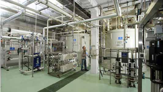
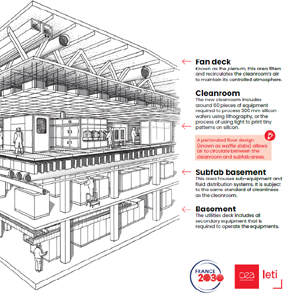
Subfabs are the infrastructure beneath the cleanroom that pump, abate and treat the gases, chemicals and wastewater chip processes leave behind. It shapes much of a fab’s environmental footprint, yet new solutions for them are hard to study inside active production fabs.
SubFAB Labs is a multi-phase program that bridges that gap with a dedicated experimental platform operated in high-volume manufacturing (HVM) mode. Partners can evaluate and qualify materials and hardware and quantify the environmental and economic benefits and scale the results to real fabs through modelling.
Pressure for this work is building. The largest chip-design companies are pushing the industry to cut its environmental footprint, and regulation of PFAS (“forever chemicals”) and their breakdown products continues to evolve. Some 20 industrial partners from across the IC value chain endorsed the SubFAB Labs initiative in a poster presented at the SEMI Google Global Executive Summit in Tokyo in 2025.
“CEA-Leti and ISRL share the conviction that the subfab, long overlooked in sustainability efforts, needs dedicated, science-based R&D. SubFAB Labs puts that conviction into practice. By activating Phase 1 on our pilot line, we are giving our partners the data they need to decide which solutions to develop, and a path to bring them from lab to fab faster,” Dauvé said.
Phase 1: Mapping What Leaves the Fab
The first phase will run for up to four years in CEA-Leti’s existing pilot line, whose wide range of technologies and processes makes it well suited to the study. It will build an exhaustive database of material-use efficiency and a catalog of the by-products of the complete family of semiconductor processes, showing which solutions the industry most needs to develop. It will also develop a reference monitoring system combining multiple sensor technologies will capture effluent composition and concentration.
First Partners
HORIBA, a maker of analytical and measurement solutions, and TOFWERK, a sensor maker, have agreed to join the initiative and as part of Phase 1 will test, validate and qualify existing and next-generation sensors on a range of IC processes at every stage of waste handling. Edwards Vacuum will use the program to deepen its understanding of process waste streams and to test real-time abatement strategies.
HORIBA, headquartered in Kyoto, Japan, offers advanced analytical and measurement solutions for a wide range of fields, including semiconductors, energy, and the environment.
“Demand is growing across the semiconductor value chain for pre-industrial testing and validation that helps manufacturers meet product goals and customer needs, as well as environmental regulations,” said Hajime Tsubouchi, Semiconductor Facility Field Leader, HORIBA. “SubFAB Labs gives us what an active fab cannot: months of continuous operation on real processes to show how our monitoring systems perform along the entire waste stream, from process exhaust to final treatment.”

TOFWERK, a Bruker company based in Thun, Switzerland, develops ultra-sensitive time-of-flight mass spectrometers for real-time chemical analysis. This technology helps chipmakers monitor and control etch and deposition processes. Through the first phase of SubFAB Labs, TOFWERK will apply this capability to process by-product monitoring under production conditions, including extended measurement campaigns to support application qualification.
“Effective abatement starts with knowing what reaches it,” said Alexander Laue, VP Emerging Technologies, Edwards Vacuum. “By mapping process by-products in detail and running for months under production conditions, SubFAB Labs gives us the data to develop and test real-time abatement strategies that respond to what each process actually emits.”
Future Phases
Four more phases, starting in 2027, will target the processes with the greatest environmental impact: PFAS treatment, etching, deposition, cleaning and polishing. Each will test prototype solutions under real manufacturing conditions, measure how much they cut emissions, and check their effects on the rest of the subfab, from waste handling and safety to cost.
Complementing Existing Initiatives
By opening an intensive experimental technology validation environment, SubFAB Labs complements the SEMI Climate Consortium and the EU GENESIS research project, which CEA-Leti coordinates.
ISRL, CEA-Leti’s partner in SubFAB Labs, is a privately held U.S. company founded in 2022 by former Intel subfab leader Ilya Zabelinsky to put subfab R&D on a scientific footing.
“Launching the first SubFAB lab in Europe is a strong start toward a global collaborative effort to solve problems no single company can address inside its own fab,” Zabelinsky said. “As the industry grows toward $1 trillion in revenue, focused, pre-competitive research is how it can keep growing and still meet its environmental targets.”
Credit: LA HACHE/CEA