Introduction
Most electronics have a power source that provides a higher voltage than the electronics’ typical working voltage. For example, a computer’s power adapter is plugged into a 110 VAC/220 VAC wall socket and draws less than one amp. After vari- ous power semiconductors perform a series of step-down voltage conversions, a computer’s processor may eventually work below 1 VDC but may consume many amps at its peak. There are many different internal voltage rails in such examples that may range from sub-1 V to 12 V.
Low dropout regulators, commonly known as LDO regulators, are used extensively in a wide variety of electronic applications to regulate and control a lower output voltage that is delivered from a higher input voltage supply. While the LDO regula- tor is often introduced at the beginning of any power management textbook and is in general considered a very simple device, a circuit designer may not well understand certain technical features that are critical in selecting an LDO regula- tor other than its voltage and current ratings. This article focuses on discussing the low noise requirement of LDO regulators, explaining other low noise power solutions, and introducing the critical applications that require low noise power.
Noise—Its Origin and How to Deal with It
An LDO regulator is rarely used directly from the power source to other circuitry—the power loss would be too large in most cases. Instead, a designer typically uses either an AC-to-DC or DC-to-DC switching regulator. As the power source (battery to AC) feeds the switching regulator, it may have its own noise and may pick up external noises that are generated by radiation and other effects in the cables or on the PCBs. To make it worse, there is never an ideal switch in such a switching regulator, and all switching events create spikes and ringing that eventually become internal noises. The switching regulator may be placed away from the load and may pick up additional external noises along its path. Quite often, an LDO regulator is added to step down the regulator output and feed the load, as the LDO regulator may provide better regulation, suppress output ripple, or there can be multiple loads that require different voltages. The LDO regulator will receive all noises fed to its input and may generate noise of its own, and all these noises could be passed on to the load if untreated (Figure 1). Since it is difficult to simulate and we cannot predict the frequency spectrum and amplitude of the noise, it may interfere with a very sensitive load circuitry (that’s why audiophiles can tell the differences in sound quality as they change power supplies). Other typical sensitive load circuitry may include radio frequency amplifiers, clock and timing ICs, SERDES, precision analog and image sensors, and such circuitry that may be found in medical equipment, test instruments, telecom, automotive, and data centers.

Circuitry designers have taken different approaches to lower the noise in their power supplies. It is helpful to add ferrite beads or low-pass filters before and after the regulators to filter the high frequency noises; however, they can be bulky and expensive. It is very painful when a designer discovers such a filter is needed after the initial design prototype is done.
A famous approach to low noise design is to use Analog Devices’ Silent Switcher® switching regulators. This product family incorporates noise-canceling technolo- gies without compromising size, efficiency, or excessive components. This family of proprietary designs has now evolved to its third generation. The first genera- tion of Silent Switcher 1 products uses a pair of switching loops in opposite polar- ity to cancel magnetic fields. The second generation integrates precision supply capacitors and eliminates PCB layout sensitivity. The third generation includes
the features of Silent Switcher 1 products, offering ultralow noise at low frequen- cies and ultrafast transient response. Silent Switcher regulators can support input voltages as high as 65 V and load currents up to 30 A and are offered as buck, boost, or buck-boost topologies. More information can be found at the Silent Switcher product page.
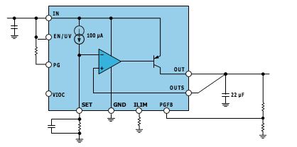
The other popular approach is to use low noise LDO regulators. A typical block diagram is shown in Figure 2. The low noise LDO regulators are designed as a precision current reference followed by a high performance voltage buffer. They are mainly characterized by three key factors: PSRR, total integrated output noise, and noise spectral density.
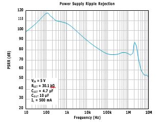
PSRR represents the fluctuations in the output voltage caused by the input volt- age (Figure 3). It is expressed in log form at a particular frequency and varies with load and input/output voltage. Essentially, as we prefer not to have the input noise reflected at the output, it is critical to use LDO regulators of high PSRR. As the high frequency PSRR can be improved by adding small low-pass filters after and before the LDO regulator, the PSRR at a lower frequency is more important in IC selection. During part selection, remember every 20 dB difference is 100× better or worse in rejecting ripples.
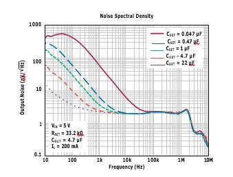
The next important figure is the noise density vs. frequency chart, as in Figure 4. There are communications-related applications with a regulation on the frequency spectrum; hence, the noise has to be controlled to pass certification testing. There are also sensor applications where the ambient signal is sensed and processed at a certain low frequency. Hence, the designers should check the spectral noise density curve around the frequency of interests.
The last important factor is the total (integrated) output noise, which is the rms value of the spectral noise density integrated over a finite frequency range. For analog-to-digital or digital-to-analog conversion circuitry, all the LDO regulator noise from DC to the bandwidth of the system is integrated together and affects the system accuracy. Hence, total output noise is important for such applications. Figure 5 shows the integrated noise of LT3045, which is quieter than a Li-Ion battery.
Compromises
For almost all applications that require at least one advanced processor and other circuitry, a complicated power supply that contains multiple output rails is required. Here the designers may choose among various options such as a PMIC (multioutput, single-chip) IC, multiple single-output regulators, or multiple LDO regulators. If low noise is required on some or all of those output rails, it becomes rather unclear on the options.
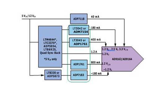
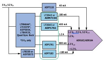
From textbooks, we can easily understand that switching regulators are in general more efficient than LDO regulators, and the LDO regulator circuitry is easier to design. In the real world, it is a bit complicated. Take ADI’s AD9162 for example. It is an IC that’s widely used in telecom and instrumentation systems. It requires a total of 10 power rails, split in 4:2:4 as analog supplies vs. digital supplies vs. SERDES supplies. While a few of these rails can be combined, we need six supplies
minimum. It is worth noticing that the analog 1.2 V is the most noise-sensitive supply on the device, followed by the analog 2.5 V and analog –1.2 V.
Here a possible approach is to use multiple Silent Switcher regulators, such as the latest released 18 V/2 A rated LT8622S or 5 V/3 A rated LTC3307B. They are most likely to meet the low noise requirement without adding external filters.
However, the system size and cost will be slightly high if all rails are powered by Silent Switcher regulators. An alternative approach that combines all the benefits like high efficiency, low cost, small solution size, and low noise is to use a PMIC and an inverting regulator as the first stage. An example is a quadruple output PMIC like LTM4644, LTC3370, ADP5054 (for 12 V bus), and LT8330/ADP5073 for the inverting regulator. Then each output rail is followed by low noise LDO regulators on all the sensitive voltage rails except for the 1.2 V VD (Figure 6).
ADI also offers Silent Switcher quad output PMICs like LT8692S, LT8686S, LT8685S, and LT7200S, if a higher voltage or higher current rating is desired.
A designer may also consider keeping the low noise LDO regulators on 3.3 VI/O and –1.2 VA and replacing the PMIC and following LDO regulators with four single- channel Silent Switcher regulators.
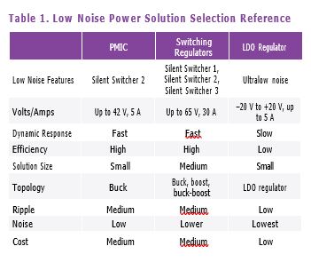
To summarize the selection criteria, a designer may refer to Table 1 for low noise solutions. In general, ADI recommends using ultralow noise LDO regulators when the input source can be very noisy, when the load current is low, when lowest output ripple is desired, or when the lowest noise is desired.
For a load current of 5 A+, almost exclusively a low noise PMIC or switching regula- tor is preferred among designers (although LDO regulators may be paralleled to support high current too).
For load current of 2 A to 5 A, it is at each designer’s discretion to choose between LDO regulators like ADP7158/ADP7159, LT3073, MAX38907, or a variety of Silent Switcher regulators.

The Applications
ADI is a market leader in low noise LDO regulators. The portfolio is further strengthened after the recent acquisition of Linear Technologies and Maxim Integrated. ADI now has a wide portfolio from –20 V to +20 V rating, and from 100 mA to 5 A, of ultralow noise LDO regulators.
Out of hundreds of customers, here are some typical application examples:
▶ A famous DSLR camera manufacturer chose low noise LDO regulators to power
its image sensors due to the ultralow noise required to process sensor signals
▶ An Amazon best-selling thermal camera maker chose low noise LDO regulators to power its infrared sensors, as they are the lowest noise solution found on the market
▶ An automotive Tier 1, advanced driver assistance system (ADAS) customer chose low noise LDO regulators to power its radar and RF circuitry (ADI also provides entire AEC-qualified power solutions to that customer)
▶ An endoscope customer chose a low noise LDO regulator for low noise and small solution size
▶ A semiconductor automatic test equipment (ATE) customer chose ADI power modules and LDO regulators to power its ASIC
▶ A gaming headphone customer chose low noise LDO regulators to power its audio DAC
▶ A printer customer chose low noise LDO regulators due to low ripple requirement
▶ A flow meter customer chose low noise LDO regulators due to high PSRR and low ripple nature
▶ A massive MIMO customer chose low noise LDO regulators to power its GaN power amplifier
In general, the low noise power supply is critical to most sensitive applications, and designers have told us that they would rather choose low noise power ICs by default to provide extra margin in their designs. If you run into any interference problem in your design, perhaps check with the power supply first.
The Future of Advanced LDO Regulators
ADI has a wide range of ultralow noise, ultrahigh PSRR LDO regulators. ADI also designs and sells hundreds of other LDO regulators of various features like high breakdown voltage, low quiescent current, and adaptive pin to allow upstream DC-to-DC to track LDO regulator load, etc. Still, the market calls for better LDO regulators with more features on a regular basis. We have customers calling on us for LDO regulators of even lower noise, multiple channels, digital configurability, faster transient response, and all sorts of ideas. While it still looks like a simple device, LDO regulators will never fade away and will keep evolving just like all the other semiconductors. For any questions or support needed, feel free to consult an ADI sales office that is closest to you. Please see the LDO Linear Regulators Parametric Search and the LDO Plus product portfolio, which includes LDO regula- tors with additional functionality.

About the Author
Zhihong Yu is currently a product marketing director at Analog Devices. He has 16+ years of professional experience in the power management, analog and mixed-signal semiconductor industry. He has led the definition and development of over 40 integrated circuits. Before ADI, he worked at Renesas Electronics, Monolithic Power Systems, and Infineon Technologies on different engineer- ing and business functions.


