Space electronics are tending toward increased system performance. As electronics approach physical size and performance limits, practical considerations such as wire ability, thermal management, electromagnetic compatibility, and system reliability become dominant issues in system design. Resolving such issues requires the use of sophisticated analysis and computational methods.
Introduction
In recent years, the electronics industry has discovered that the major economic advances made in high performance electronic circuitry have come with increased integration. The industry is rapidly converging toward true wafer-scale integration, i.e., toward an entire system fabricated on one silicon substrate. Every 5 years or so, we see wafer foundries processing larger silicon wafers with smaller line geometries. Today, 12- in. wafers are being processed with 0.35-µm lines. By the year 2010, 16-in. wafers and 0.10-µm lines will likely be the standard. The quest to achieve better performance (higher speed and integration) has placed pressure on manufacturers and has forced integrated circuits (ICs) closer together.
The primary objective of microelectronic packaging is to design an electronic system that will satisfy the requirements for a particular application at a reasonable cost. Because of the many options available to interconnect and house an electronic system, the choice of a packaging technology for a given application is not always straightforward. Selection criteria may include one or more technology drivers:
• Wire ability
• Yield
• Cost
• Heat transfer characteristics
• Electromagnetic performance
• Mechanical toughness
• Reliability
These basic principal design considerations affect speed, functionality, junction temperatures, volume, and weight. The primary goal is to select the most cost- effective yet reliable interconnection technology, which requires a quantification of the technology drivers. The resolution of these key design issues often depends on the use of sophisticated analysis methods.
Space Components Market Latest Insights 2024
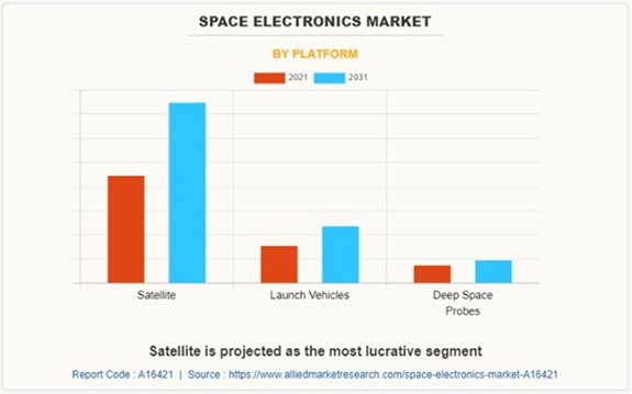
According to a report by Allied Market Research The global space electronics market was valued at $3.3 billion in 2021, and is projected to reach $5.4 billion by 2031, growing at a CAGR of 5.04% from 2022 to 2031.the growth in the historic period can be attributed to space exploration initiatives, significant investment in satellite manufacturing, increase in demand for space electronics products, rising prevalence of space operations, rising satellite launch and deep space activities.
The Space Electronics market size is expected to see strong growth in the next few years. It will grow to USD 3.5 billion in 2028 at a CAGR of 6.9%.
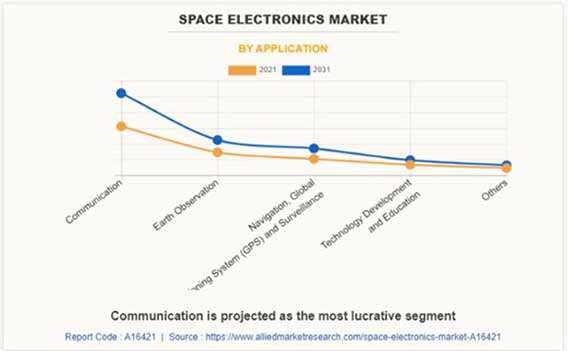
The global space electronics market is segmented on the basis of platform, application, type, component, and region. By platform, it is categorized into satellite, launch vehicles, and deep space probes. Depending on application, it is fragmented into communication, earth observation, navigation, a global positioning system (GPS) & surveillance, technology development, and education, and others. By type, it is divided into radiation hardened and radiation tolerant. By component, it is divided into microprocessors and controllers, sensors, application specific integrated circuits (ASIC), memory chips, power source and cables, discrete semiconductors, and other. Region-wise, the market is analyzed across North America, Europe, Asia-Pacific, and LAMEA.
Space electronics can be identified as electronics components such as microprocessors, controllers, memory chips, and application-specific integrated circuits (ASIC) among others that are designed and developed for application in satellites, rocket launchers, and deep space probes. These electronics are exposed to extreme vibrations, radiation, and other harsh environment in space, posing a demand for radiation treatment that allows them to operate flawlessly in harsh environments.
Additive manufacturing, or 3D printing, has been gaining popularity in the satellite industry due to its ability to produce complex parts and reduce manufacturing costs. This technology is being used to produce satellite components such as antennas, brackets, and engine parts.
These innovative technologies include high-performance electronics, advanced sensors, lightweight materials, and propulsion systems. Another trend is the increasing use of pre-existing components and subsystems commercial-off-the-shelf (COTS) in satellite design and development. COTS components can significantly reduce development time and costs while improving reliability and performance.
Challenges for Electronic Circuits in Space Applications
Space is a harsh environment with numerous challenges for electronic circuits. Component failures, outgassing, and mechanical mounting issues are just some of the challenges faced by electronic circuits in space applications.
Here are some of the space conditions that pose challenges for electronic circuits:
Pressure – There is zero pressure in space and components manufactured under atmospheric pressure may behave differently under such no-pressure conditions.
Ion and particle presence – In the space application for low earth orbits, UV radiation causes molecular degradation of helium, oxygen, nitrogen, etc. The atomic versions of these elements initiate corrosion and erosion of materials. The ions and free electrons in space can cause arching, which may affect sensitive electronic components.
UV degradation – UV degradation changes the composition of materials and can even remove oxygen from materials, thereby affecting the performance of the components.
Radiation – The free-particle radiation environment can introduce single-event glitches that may challenge the operation of sensors and controls in electronic circuits.
Extreme temperature and thermal cycles – Extreme hot and cold temperatures and thermal cycles impose mechanical stress on electronic components, especially ICs and their packages.
Apart from the conditions in space, vibration during the launch of a space system is the main reason for the failure of space electronic circuits.
Component Packaging solutions in the semiconductor market
As curiosity and innovation drive space exploration forward, constraints for size, weight and power continue to tighten. To design for space, we have no room for error. And increasing space exploration activities by public and private entities, requires continued collaboration and improvements.
According to European Space Agency the Hybrids and Packaging domain cover all types of EEE components, addressing the construction and performance of devices used for satellite electronics applications.
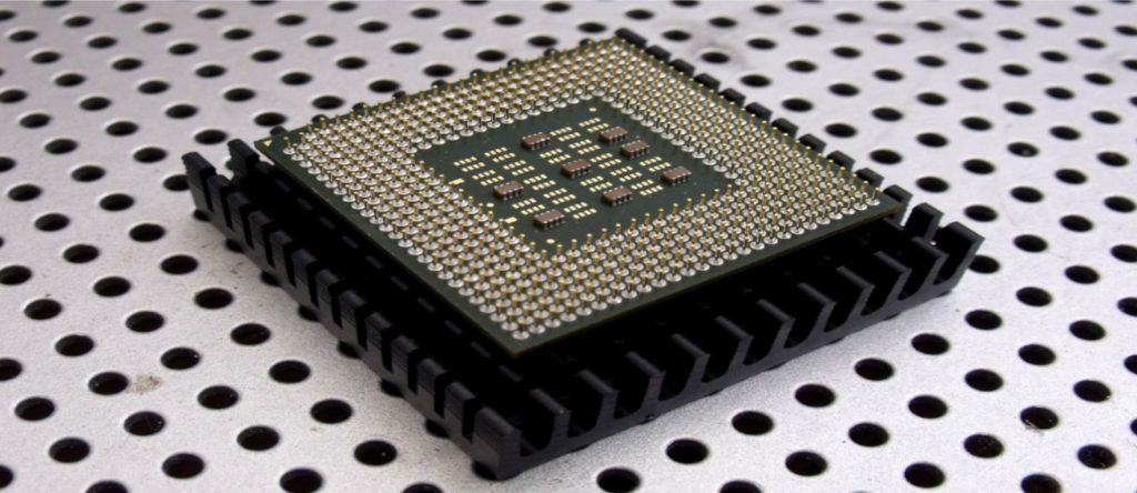
Included within the perimeter are:-
- Hermetic hybrids – generally complex multi-chip devices, with a ceramic substrate, enclosed in a hermetically sealed package.
- Non-Hermetic packages – devices that may be complex with a variety of substrate materials and types, that include semiconductor devices but are not sealed within hermetic cavities.
- Discreet device packaging of Silicon, Gallium arsenide and Gallium Nitride.
- Assembly of devices using Chip on Board technologies.
Authentic packaging is essential as it serves the function of complaint and connecting the functional elements (transistor, MMIC, ASIC, etc.) to the rest of the electronic assembly. Reliable packaging must need the right combination of materials and the highest quality in manufacturing processes.
Future packaging developments such as COTS, 2.5D & 3.0D devices & Non-hermetic products will offer cost and technological benefits. Understanding, developing and ensuring the reliability of these developments is of critical importance for future missions.
QML Class P packaging standard enables more advanced computing in space, such as how satellites and other spacecraft can autonomously process data and make decisions in orbit as opposed to beaming data back down to Earth,” said Javier Valle, product line manager for space power Texas Instruments. “More processing capability also requires greater power. With TI’s QML Class P portfolio, TI increase the efficiency of the power supply while reducing the size of the overall package, resulting in much higher power density.
TI’s QML Class P certified portfolio offers solutions across the entire spacecraft electrical power system (EPS), from solar panels all the way to point of load power supplies, and the portfolio is growing.
QFN (quad flat no-lead) and BGA (ball grid array) dominate the semiconductor market with >50% market share, and further analysis by Alter Technology Group shows that European customers are regularly submitting commercial off-the-shelf COTS devices in QFN packages devices for up screening evaluation to ECSS-Q-ST-60-13C. QFN and BGA are flexible platforms that can be serviced with common block mold tooling and saw singulation. Soldering techniques and PCB materials are being adapted to cope with leadless packages, previously undesirable for space applications.
Flip Chip Assembly Process
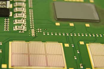
Flip chip assembly is an efficient and reliable way to assemble components onto a PCB. It is a cost-effective option that can be automated for large production runs, making it ideal for use in a variety of industries.
Flip chip assembly techniques bring a wide range of benefits:
- A reduced parasitic interconnection between the semiconductor die and package.
- Provides a high final assembly integrity density.
- Minimize the interconnection length, providing better electrical performances, especially for high-speed signals.
- Reduce device size and weight etc.
Electronic, and electromechanical (EEE) parts shielding
Use of more effective shield material lowers the predicted mission TID level seen by a part. There are better than aluminum materials (like tantalum), and there are more effective shielding techniques (like multilayer shields). Active shields (like magnetic) are in research stage.
Radiation Induced Latch Up (SEL)
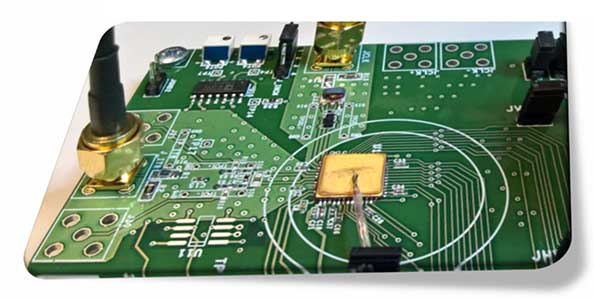
The mitigation consists of a latch up protection circuit to quickly disconnect the damaging current. To implement such a mitigation, the latch up current shall be known from the SEL testing.
The SEL Testing is performed in heavy ions accelerators and involves high cost and a long time. In order to reduce cost and time, the following issues should be revisited:
SEL test method
Another SEL Test Method, worth being considered, is the less expensive Pulsed Laser SEL (and other SEE) testing, proved as efficient. By the way, the pulsed laser source may play an important role in bit mapping, mitigating Multiple Bit Upsets (MBU). Another known SEL Test Method is Californium 252, if used within its limitations.
Part technology/process
To help the rather complicated, difficult task of COTS SEL assessment the following information is needed: technology, process, foundry, and die revision. Alliances in the space industry can substantially contribute to avoid testing duplications.


