Electronics Era

  • About Us
  • Advertise with Us
  • Contact Us
  • e-Mag
  • Webinars
Header logo on website
Advertisement
Advertisement
Menu
  • News
    • Industry News
    • Product News
  • TECH ROOM
    • Sensor
    • VR / AR
    • Embedded
    • Medical Electronics
    • Industry 4.0
    • Robotic
    • Automation
    • Smart Machine
    • Component
    • Manufacturing
    • Aerospace & Defence
    • Security
    • Policy
  • Semiconductor
    • AUTOMOTIVE ELECTRONICS
      • EVs
      • HEVs
      • ADAS
      • Connected Cars
    • IoT-Internet of Things
      • Development Kit
      • IoT Design
    • Power Electronics
      • AC-DC/DC-DC Converters
      • Mosfets
      • IGBTs
      • LEDs
  • T & M
    • 5G testing
    • Oscilloscopes
    • SDN & NFV
    • RF & Wireless
  • AI/ML
  • Telecom
    • 5G/6G
  • RENEWABLES
    • Sustainability
  • Future Tech
    • Data Center
    • Cloud Computing
    • Big Data Analytics
  • Webinars
  • Editor’s Pick
    • Tech Article
    • Tech Blog
    • White Papers
    • EE-Tech Talk
    • Market Research
  • EE Awards
    • EE Awards 2025
    • EE Awards 2024
  • MORE
    • E-Mag
    • Events
    • Subscription
    • Contact Us
Home Semiconductor

Deca and Silicon Storage Announce Strategic Collaboration to Enable NVM Chiplet Solutions

The collaboration provides customers with a modular, memory-centric foundation for advanced multi-die architectures

Editorial by Editorial
September 11, 2025
in Semiconductor
Reading Time: 3 mins read
SST and Deca
Share on FacebookShare on TwitterShare on LinkedIn

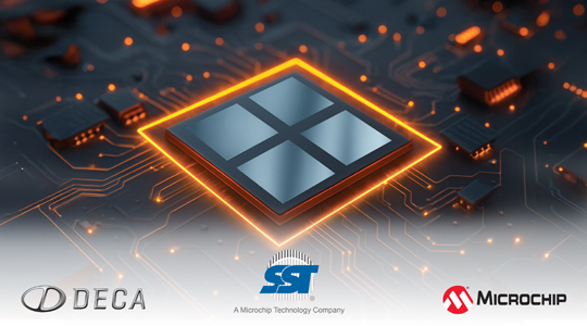
As traditional monolithic chip designs grow in complexity and increase in cost, the interest and adoption of chiplet technology in the semiconductor industry also increases. Deca Technologies and Silicon Storage Technology® (SST®), a subsidiary of Microchip Technology Inc., announced today that they have entered into a strategic agreement to innovate a comprehensive non-volatile memory (NVM) chiplet package to facilitate customer adoption of modular, multi-die systems.

This collaboration combines Deca’s M-Series™ fan-out and Adaptive Patterning® technologies with SST’s industry-leading SuperFlash® embedded flash technology.  The companies are applying their system-level integration expertise to deliver a bundled offering that empowers customers to design, verify and commercialize NVM chiplets. By enabling greater architectural flexibility, the solution offers both technical and commercial advantages over traditional monolithic integration.

The collaborative solution provides a modular, memory-centric foundation for advanced multi-die architectures by combining the strengths of both companies. The chiplet package leverages SST’s SuperFlash technology, along with the interface logic and physical design elements required to function as a self-contained chiplet. This is paired with Adaptive Patterning-based redistribution layer (RDL) design rules, simulation flows, test strategies and manufacturing paths through Deca’s ecosystem of qualified partners.

Building on this foundation, Deca and SST will jointly support customers from early design through qualification and prototype manufacturing. By streamlining integration and accelerating design cycles, the companies aim to enable broader adoption of heterogeneous integration, engaging with customers globally to bring chiplet solutions to market.

“Chiplet integration is reshaping how the industry thinks about performance, scalability and time to market,” said Robin Davis, VP of Strategic Engagements & Applications at Deca. “Our partnership with SST empowers customers to develop a chiplet solution that combines different chips, process nodes, sizes and even die from multiple foundries delivering more efficient and cost-effective products.”

Chiplet technology offers significant advantages in semiconductor design and manufacturing by enabling a more-than-Moore approach. Designers can go beyond traditional scaling to deliver enhanced functionality and performance and get products to market faster. Chiplets allow the reuse of existing IP and can facilitate the mixing of advanced process nodes with less expensive legacy geometries. By utilizing the most appropriate die technology for a particular function, chiplets provide a versatile, efficient and economical pathway for advanced semiconductor innovation.

“As our customers push the boundaries of Moore’s Law, they are expressing greater interest in chiplet- based solutions,” said Mark Reiten, Vice President of Microchip’s licensing business unit. “This partnership aims to deliver a comprehensive package of IP, simulation tools and advanced assembly and engineering services necessary for successful chiplet development and productization.”

Pricing and Availability

Customers interested in SST’s SuperFlash technology should access the SST website or contact a regional SST sales executive for more information and details of our NVM chiplet solutions. Those interested in Deca’s technology and offerings should visit the Deca website or reach out to Deca’s marketing contact.

For more information, visit the Microchip website at www.microchip.com.

Tags: DecaNVM ChipletSilicon Storage
Editorial

Editorial

Join Our Newsletter

* indicates required
Electronics Era

Electronics Era, India's no.1 growing B2B news forum on Electronics and Cutting Edge Technology is exploring the editorial opportunity for organizations working in the Electronics Manufacturing Services(EMS) Industry.

Follow Us

Browse by Category

  • 5G testing
  • 5G/6G
  • AC-DC/DC-DC Converters
  • ADAS
  • Aerospace & Defence
  • AI/ML
  • Automation
  • AUTOMOTIVE ELECTRONICS
  • Big Data Analytics
  • Blockchain
  • Cloud Computing
  • Component
  • Connected Cars
  • Data Center
  • Editor's Desk
  • EE-Tech Talk
  • Electronics Components
  • Embedded
  • EVs
  • Future Tech
  • HEVs
  • Industry 4.0
  • Industry News
  • IoT-Internet of Things
  • LED & Lighting
  • LEDs
  • Manufacturing
  • Market Research
  • Medical Electronics
  • Mosfets
  • News
  • Oscilloscopes
  • Policy
  • Power Electronics
  • Product News
  • RENEWABLES
  • RF & Wireless
  • Robotic
  • SDN & NFV
  • Security
  • Semiconductor
  • Sensor
  • Smart Machine
  • SMT/PCB/EMS
  • Sustainability
  • T & M
  • Tech Article
  • Tech Blog
  • TECH ROOM
  • Telecom
  • Uncategorized
  • VR / AR
  • White Papers

Recent News

Towards Automotive

Driving the Future of Mobility with Automotive Connectors

September 11, 2025
Würth Elektronik

Würth Elektronik stages its virtual conference from October 20 to 23

September 11, 2025
  • About Us
  • Advertise with Us
  • Contact Us

© 2022-23 TechZone Print Media | All Rights Reserved

No Result
View All Result
  • News
    • Industry News
    • Product News
  • TECH ROOM
    • Sensor
    • VR / AR
    • Embedded
    • Medical Electronics
    • Industry 4.0
    • Robotic
    • Automation
    • Smart Machine
    • Component
    • Manufacturing
    • Aerospace & Defence
    • Security
    • Policy
  • Semiconductor
    • AUTOMOTIVE ELECTRONICS
      • EVs
      • HEVs
      • ADAS
      • Connected Cars
    • IoT-Internet of Things
      • Development Kit
      • IoT Design
    • Power Electronics
      • AC-DC/DC-DC Converters
      • Mosfets
      • IGBTs
      • LEDs
  • T & M
    • 5G testing
    • Oscilloscopes
    • SDN & NFV
    • RF & Wireless
  • AI/ML
  • Telecom
    • 5G/6G
  • RENEWABLES
    • Sustainability
  • Future Tech
    • Data Center
    • Cloud Computing
    • Big Data Analytics
  • Webinars
  • Editor’s Pick
    • Tech Article
    • Tech Blog
    • White Papers
    • EE-Tech Talk
    • Market Research
  • EE Awards
    • EE Awards 2025
    • EE Awards 2024
  • MORE
    • E-Mag
    • Events
    • Subscription
    • Contact Us

© 2022-23 TechZone Print Media | All Rights Reserved

Advertisement
Advertisement