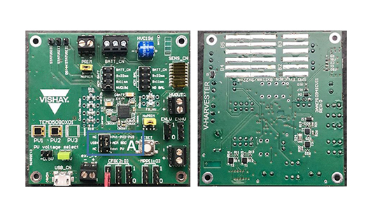
Fig. 1 – V-harvester board
DESCRIPTION
The V-harvester board is a photovoltaic (PV) harvesting backup demonstration circuit. It is a sophisticated stand-alone board charged using TEMD5080X01 micro PV cells or with micro USB. The input power goes into an e-peas low power AEM10941 controller, where it is stepped up to the supercapacitor voltage of 4.2 V. Upon power demands at the interface or ENLV, ENHV settings, the controller converts the supply voltage to the target voltages using low dropout regulators (LDO).
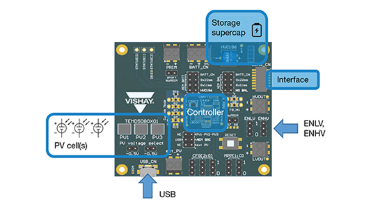
These target voltages are set to 1.8 V (low voltage) and 2.5 V (high voltage) on this board by a high ohmic resistor network. The board is equipped with a 4 F / 4.2 V 196 HVC ENYCAP™ hybrid energy storage capacitor, and has options to jumper to other storage capacitors on the backside (or a BATT_CN = battery connector).
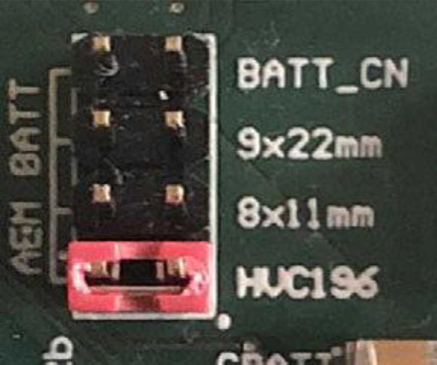
Fig. 2 – Jumper AEM_BATT set to 196 HVC ENYCAP™ (by default populated as 4.2 V / 4 F)
If faster charging is needed, an external PV cell can be connected (and jumpered). If no light harvesting is available, jumper A can be set to USB.

Fig. 3 – AEM SRC set to PV1-3, or AEM SRC set to USB
Upon connection of a 5 V micro USB cable, the red LED close to the USB port turns on and the “Status 2” green LED will flash once every ~ 5 seconds.
LIFE WORKING SIGNAL
The green Status 2 LED indicator is available to view as a periodic life signal. This indicator is active – even if AEM SRC is jumpered to sources other than USB – to visualize operation. However, as described in the last section, only if USB is connected. This means the power to flash this indicator is drawn from USB only and will not consume power otherwise. Status 2 is the MPPT signal by the controller and is always active, even in very dark conditions. If the indicator does not flash periodically, then the PV cell boost circuit was shut down by a PV input voltage below 50 mV. To reactivate it, an initial trigger of at least 400 mV PV voltage or a kick-start by a USB input source – including jumper USB to AEM ARC – is required.
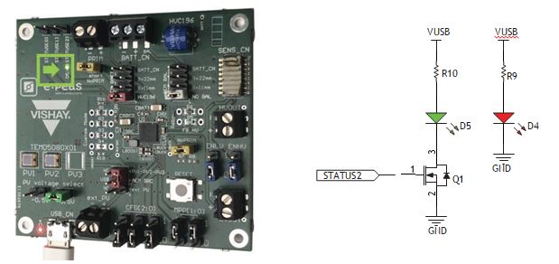
Fig. 4 – Status 2 green LED indicator (actually flashing) + RED LED to indicate USB port power
MINIMAL JUMPER SETTINGS
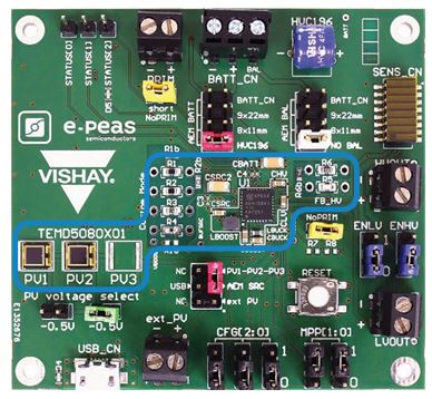
- Yellow jumpers “PRIM / NoPrim” for no primary cell attached
- Green jumper “-0.5 V” for PV setting, as described in the next paragraph (pictured is one possibility)
- AEM Batt setting to any of the sources (here, an upper red jumper to the 196 HVC)
- AEM SRC setting either to PV or USB (here, the lower red jumper to PV1 – PV3)
- CFG2 [CFG[2:0] left] set to zero to define the 1.8 V and
2.5 V default settings (custom voltage defined by resistors) (black jumper)
The minimum for activating the low voltage 1.8 V output is setting the ENLV jumper to 1 (blue jumper).
The minimum for activating the high voltage 2.5 V output is setting the ENHV jumper to 1 (blue jumper).
The ENHV can be controlled from the SENS_CN interface too.
PHOTOVOLTAIC HARVESTING ELEMENTS
The board is equipped by default with two PV cells, and the target input should be jumpered with the green jumper JP4 shown above to bypass PV3.
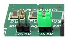
The schematic for the configuration is:
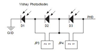
The term “-0.5 V” refers to the possibility of subtracting 0.5 V in direct sunlight if operation with fewer PV cells than populated is tested. The right jumper is required if two PV cells are populated.
PV RESPONSE OF THE TEMD5080X01
The silicon PIN photodiode is a blue enhanced version of many other Vishay PIN photodiodes of the same size. It has an effective sensitive area of 7.7 mm2 and can deliver up to 2 mA at direct sunlight and 1.5 AM.
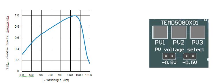
Fig. 5 – Relative spectral sensitivity vs. wavelength
Measurements were carried out with a 100 W incandescent light bulb and a dimmable office LED bulb to replicate cloudy / sunny weather.
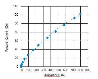
Fig. 6 – 100 W incandescent light bulb (max. 120 μA at 800 lx)
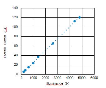
Fig. 7 – LED – 2700 K 45 mA dimmable (max. 120 μA at 4800 lx)
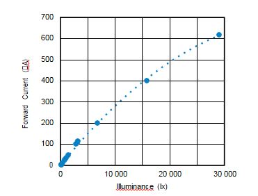
Fig. 8 – PV response at direct sunlight
VOLTAGE SETTINGS
The high ohmic voltage divider is composed of resistors, which in total do not consume more than 0.1 μA of power. This includes the following resistors:
- RCWP040220M0FKEC – 0402 1 % thick film 20 ML – industrial / high reliability
- MCT06030C1005FP500 – 0603 ± 1 % thin film 10 ML, professional thin film chip resistors
The voltage divider is optimized for long lasting IoT operational life.
In the following designators:
- R1 is made of series R1 and R1b
- R2 is made of series R2 and R2b
- R6 is made of series R6 and R6b to accomplish the target values
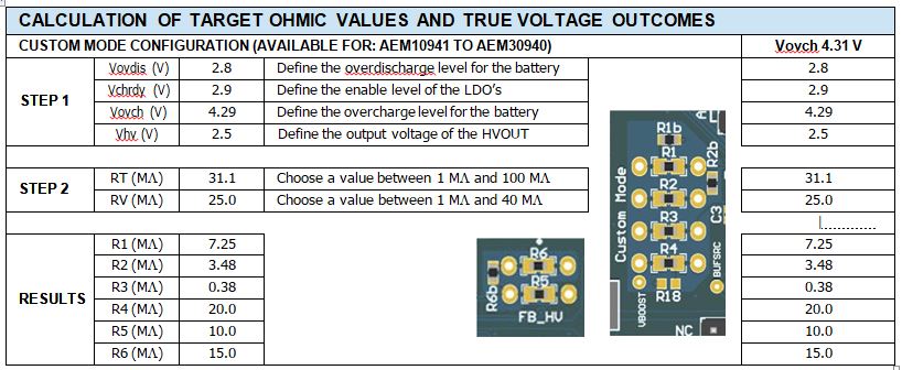
This table shows the ideal values in column 3 and the used values in the last column to accomplish the following voltages:
- Minimum voltage for the storage capacitor = 2.8 V
- Enable voltage level for the HV LDO = 2.9 V (HV is generated by the LDO from the storage capacitor voltage)
- Maximum voltage for the storage capacitor = 4.29 V
- High voltage output level = 2.5 V
The results are R1 to R6, which are in total 55 ML attached to the Vboost regulator output. The LV 1.8 V output is the default (see next table).
OTHER VOLTAGE SETTINGS
Other voltages than the resistor network defined are possible with the CFG0 to CFG2 jumpers.

The custom mode Voch means V = 4.29 V as a cut-off charge voltage, as defined in the 196 HVC ENYCAP™ datasheet. Do not jumper CFG1 to one unless jumpered to a source other than the 196 HVC ENYCAP™ at AEM BATT!
Vchrdy means that from this voltage on, the LDOs will work on this board by resistors defined to V = 2.9 V (assuming a dropout of the HV LDO has enough margin to power up to 80 mA at 2.5 V).
Vovdis means a discharge cutoff voltage of the controller (entering shutdown), but on this board by resistors defined to V = 2.8 V. Assuming no LDO is being used, the 196 HVC is not to be used below this voltage level and is therefore waiting to be reset or kick-started by a USB port charge or other source current trigger. The RESET button on the board is only required if CFG jumpers are modified and the resistor network is modified, e.g., to open or other values. By default, resistors are present which define all voltages.
LOW VOLTAGE AND SHUT DOWN PROCEDURES
There is an operation in place below the 2.8 V ENYCAP™ voltage, down to 1.9 V, for PV charging and MPPT. The operation of this can be tracked by attaching a USB source, but keeping the AEM SRC jumper to PV1-3. Then the green Status 2 LED would still blink (if the system came from deep sleep or zero, a PV voltage of at least 400 mV is required to start again).
Below the ENYCAP™ voltage of 1.9 V, the device enters a deep sleep state, waiting for a current source trigger or a bright enough light condition for the PV cell to start the controller again. This is typically at around a 400 mV PV input voltage. More details on this can be found in the datasheet of the AEM10941 from e-peas.
INTERFACE CONNECTOR SENS_CN
The interface connector on the board was routed to the best of many possibilities, with the aim of fitting the SensorXplorerTM boards provided by Vishay.
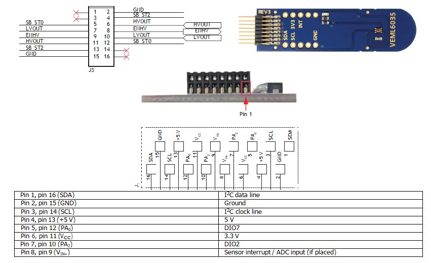
Possible Implementation Guide
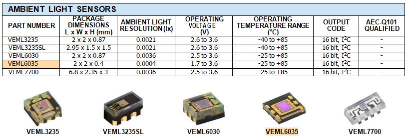
Since most sensors from Vishay will fit voltages of 1.7 V and 2.5 V in the future, the following backwards compatibility was chosen as a best fit (also because on most current daughter boards only the following pins are connected: GND, VCC, SCL, and SDA). The VEML6035 low power, high sensitivity I2C ambient light sensor, for example, is a board that requires minimum operating voltage 1.7 V only. Others require 2.5 V at a minimum.
Pin 7 / pin 10 is an input on the SensorXplorer mainboard (which does not interfere with providing 1.7 V here) and is not used / connected on any sensor daughter board pin.
Pin 8 / pin 9 is an input on the SensorXplorer mainboard (which does not interfere with a logic switching ON the 2.5 V high voltage). It can be demanded by a future sensor daughter board with a low voltage microcontroller permanently running and switching ON its sensor component, which normally requires a higher voltage than 1.8 V upon sampling, e.g., for infrared emitters, humidity sensors, proximity sensors, or RF transceivers.
Pin 4 / pin 13 is a 5 V input line to some sensor daughter boards and does not interfere with providing a periodic Status 2 signal. For future implementations, this is a periodic life or trigger signal (once every 2 s to 3 s) from the V-harvester board. Then a running RTC on a future daughter board is not required to wake up periodically. Instead, the Status 2 port trigger wake-up can be used.
Pin 6 / pin 11 are the main 2.5 V output (similar to the main VCC = 3.3 V on the daughter boards), which can be enabled manually from the V-Harvester board.
SIZE OF A MINIMAL IMPLEMENTATION
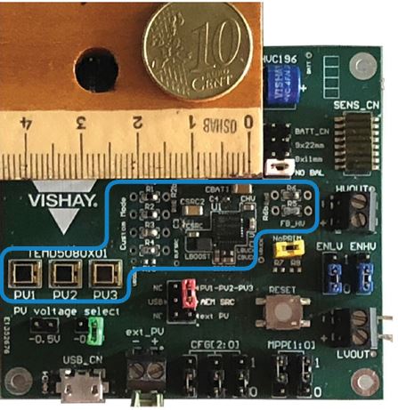
Fig. 9 – Visualization of component sizes
The total minimal size of an IoT sensor can be built with a base circuit around the controller chip totaling 12 mm x 12 mm =
~ 150 mm2. It is recommended to use at least two PV cells with 2 x 5 mm x 4 mm = 40 mm2. The 196 HVC ENYCAP™ has outer dimensions of 7.5 mm x 7.5 mm = ~ 60 mm2.
With 10 % margin and spacing around, the total size of a circuit can be as small as 250 mm2 x 1.1 = 275 mm2.
The implementation would then have 13.8 Ws of storage energy and could harvest 2 mW average in direct sunlight. Output power can be as a high as 2.5 V at 80 mA = 200 mW peak pulse power, and 25 mA as the maximum continuous current presented by the 196 HVC ENYCAP™ 4 F, 4.2 V capacitor.
MEASUREMENT
With a PV cell as the input power – but with several tracking, maximizing effects (e.g. MPPT), and monitoring tasks triggered periodically and sometimes at the same time – input and output power are dynamic. Therefore, it is difficult to calculate efficiencies at a specific point in time.
The follow measurements were done with an external PV input.
Case 1: Equilibrium
3 x PV (3 x 0.4 V); the only equilibrium setup found (1)

Notes
(1) Equilibrium state means a stable condition with a constant ENYCAP™ voltage
(2) This ENYCAP™ is under development, but was chosen because its capacitance of 0.2 F shows whether the voltage is rising or decaying much better
The following three measurements (case 2 to 4) include an ENYCAP™ voltage rising or falling, and therefore the input / output is added / subtracted to / from the energy balance and calculation.
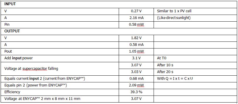
Case 2
Voltage at supercapacitor used as additional input; 1 x PV cell
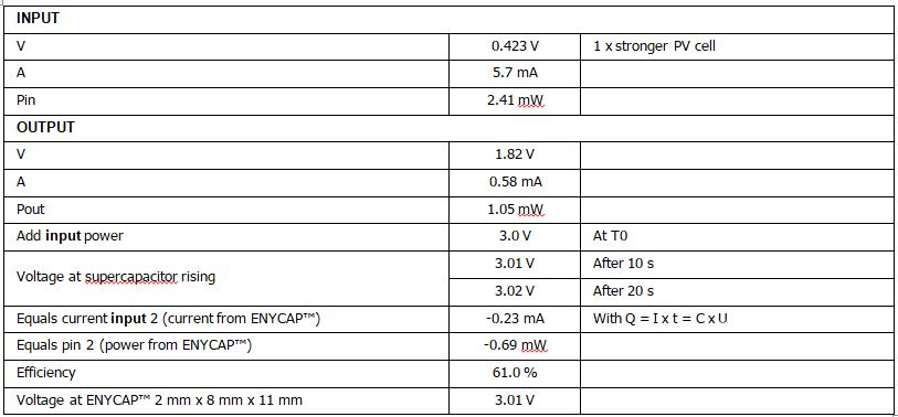
Case 3
Voltage at supercapacitor used as additional input (power); like 2 x PV cell
Case 4
Voltage at supercapacitor used as additional output (output means power is used to charge the supercapacitor).
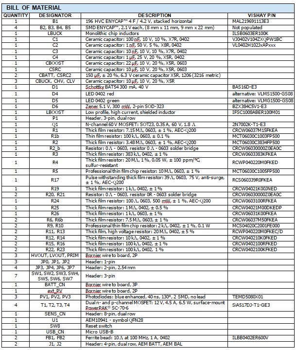
The conversion efficiency is always calculated as the ratio: input PV to LDO output 1.7 V.
PRECAUTIONS
ABSOLUTE MAXIMUM RATINGS
Any input pin 5.5 V
Operating temperature -20 °C to +85 °C
Storage temperature -40 °C to +85 °C
Primary cell input should be between 0.6 V and 5 V.
Do not connect the jumper “short no PRIM” if a primary cell is attached. This short circuits the header PRIM. Do not jumper CFG1 to one unless jumpered to a source other than the 196 HVC ENYCAP™ at AEM BATT!
External PV
An external PV cell can be of any voltage up to 5 V max. Dark periods will not discharge the storage element.
INCLUDED MATERIALS
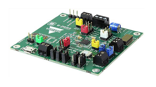
V-Harvester Board
- Board: 64 mm x 69 mm
- Set of jumpers
- This document link to the product specification: www.vishay.com/doc?28496
- 196 HVC ENYCAP™ product specification: www.vishay.com/doc?28409
LINKS
- Batteryless IoT Sensor Telecommunications Applications | Vishay
origin-www.vishay.com/applications/telecommunications/batteryless_iotsensor/
- Vishay – Engineer’s Toolbox
origin-www.vishay.com/landingpage/et4/et3te_iot1.html
- SensorXplorer™ www.vishay.com/landingpage/SensorXplorer/
CONTACTS
- If you need further information about storage capacitors, please contact: hybridstorage@vishay.com
- If you need further information about photo PIN diodes, SensorXplorer boards, ambient light sensors, and proximity sensors, please contact: sensorstechsupport@vishay.com
If you need further information about this reference design and circuit design support, please contact: iot.sensors@vishay.com
Thank you for using and buying the V-harvester board!


