Abstract
48 V distribution is popular in data center and communication applications, with many different solutions for the step down from 48 V to the intermediate rail. The simplest approach could be a buck topology, which can provide a high performance but often falls short in power density. Upgrading the multiphase buck with coupled inductors enables a dramatic power density improvement that matches the state-of-the-art alternatives while keeping the massive performance advantage. The multiphase coupled inductors have inverse coupling between windings that enables current ripple cancelation in each phase current. This benefit can be traded either for efficiency or, for example, size reduction and improvement of the power density. This article illustrates an example with 4× reduction in magnetics volume and weight, allowing an industry standard size of 1/8 of the brick for a 1.2 kW solution with peak efficiency above 98%. This article also focuses on how to optimize the 48 V topology based on the figure of merit (FOM) of the coupled inductors. It will be of interest to engineers focusing on the DC-to-DC con- version area.
Introduction
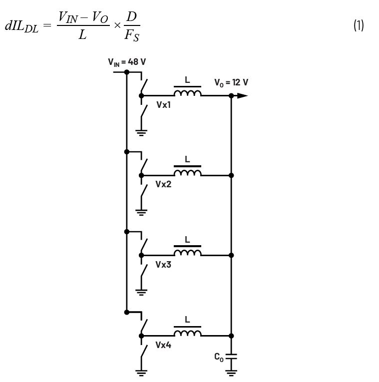
The 48 V distribution rail is typically stepped down to some intermediate voltage, often 12 V or lower, and then the different local point-of-load regulators deliver a variety of different voltages directly to different loads. One of the first choices to consider for the step-down voltage regulator 48 V to 12 V is a multiphase buck converter (Figure 1). This is a solution with regulated VO and fast transient, which is simple and inexpensive to implement. For a power range of a few hundred watts to >1 kW, four parallel phases can be considered. However, as high efficiency is often a priority: switching frequency is often relatively low for the 48 V kind of converters to keep the switching losses down, as compared to the lower voltage applications with 12 V or even 5 V input. This hurts magnetics twice in terms of volt × seconds, as the already noticeable voltage is also applied for a relatively longer time. As a result, magnetics for 48 V are typically bulky, with multiturn windings to withstand the significantly increased volt × seconds as compared to lower voltage applications. High efficiency can still be achieved in 48 V buck converter, but typically with a significant overall size, where inductors occupy most of the volume.
The basic 48 V to 12 V ~1 kW buck converter has four phases with discrete inductors 6.8 μH and switches at 200 kHz. These four inductors are by far the biggest and tallest components, representing a majority of the solution volume. The objective of the article is to keep or improve the achieved high efficiency of this initial design but reduce the size of the magnetics significantly.
The current ripple in each phase of the conventional buck can be found as Equation 1, where the duty cycle is D = VO/VIN, VO is the output voltage, VIN is the input voltage, L is inductance value, and Fs is the switching frequency.
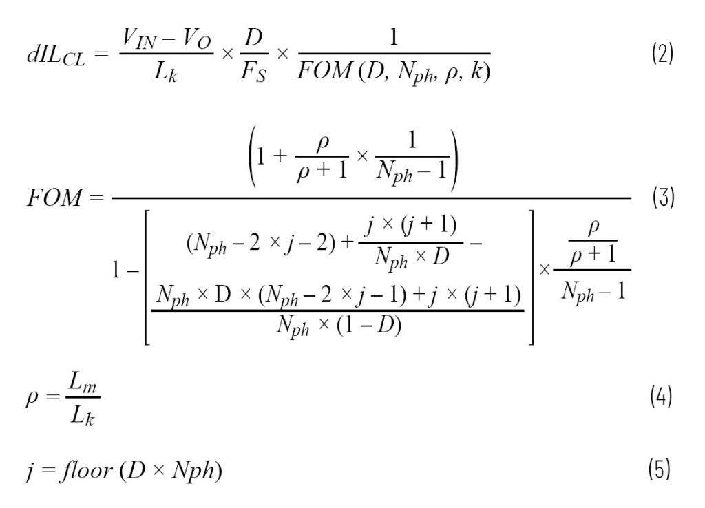
Replacing the discrete inductors (DL) with the coupled inductor1–7 that has a leak- age inductance Lk and the mutual inductance Lm, the current ripple in CL (coupled inductor) can be shown as Equation 2.6 The FOM is expressed as Equation 3, where Nph is the number of coupled phases, ρ is a coupling coefficient (Equation 4), and j is a running index, which just defines an applicable interval of the duty cycle (Equation 5).
CL Considerations
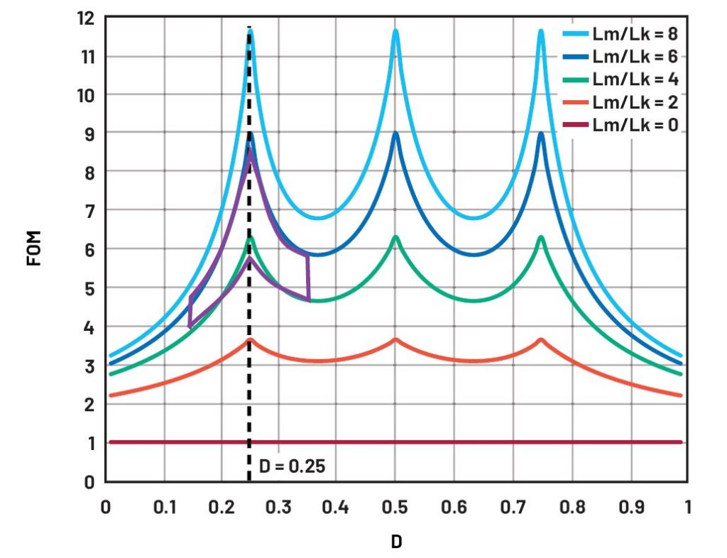
The first step for the improvement would be to plot a FOM for the Nph = 4, for several practically reasonable values of the coupling coefficient Lm/Lk (Figure 2). The red curve Lm/Lk = 0 represents FOM = 1 baseline for the discrete inductor. It was shown that the notch CL (NCL) structures with very low leakage can generally achieve very high Lm/Lk and therefore high values of FOM.8,9 However, while the duty cycle of interest is ideally right in the first notch D = 12 V/48 V=0.25: it is necessary to consider some range for the VIN and also VO. Sometimes the nominal VIN can be 48 V or 54 V plus some tolerance, VO can be adjusted away from 12 V, and so on. In order for the current ripple to remain contained if the duty cycle changes around D = 0.25 in some range, a typical CL design with significant leakage is chosen instead of NCL, still with a significant FOM value. Assuming Lm/Lk > 4, a benefit of ~6× could be considered from FOM in Figure 2 to decrease the inductance value in CL, compared to the DL baseline. Decreasing the energy storage should directly affect the required volume of the magnetics. Reducing DL = 6.8 μH value to CL = 1.1 μH should therefore be beneficial for the size reduction.
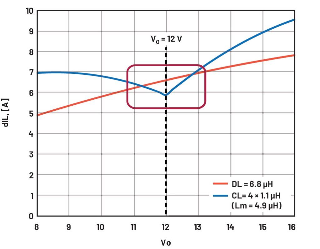
The corresponding current ripple is plotted in Figure 3, comparing baseline design DL = 6.8 μH with proposed 4-phase CL = 4 × 1.1 μH (Lm = 4.9 μH) at VIN = 48 V and Fs = 200 kHz conditions. In the region of interest, the current ripple of CL is similar to or smaller than that of DL. This implies that rms of all circuit waveforms is similar and so are the conduction losses. Same ripple at the same Fs also implies the same switching losses, gate drive losses, etc., which means that the efficiency between the two solutions should be very similar (assuming a similar contribution from DL and CL inductor losses, as the only difference).
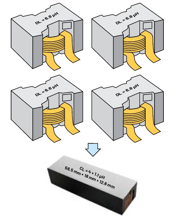
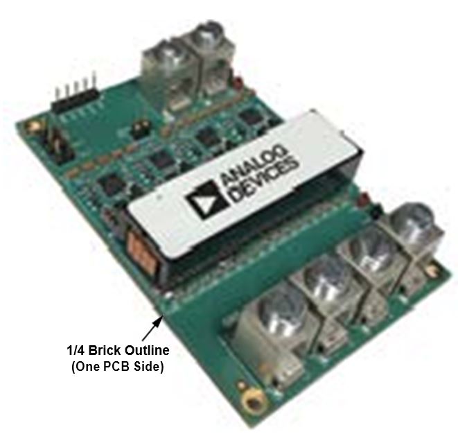
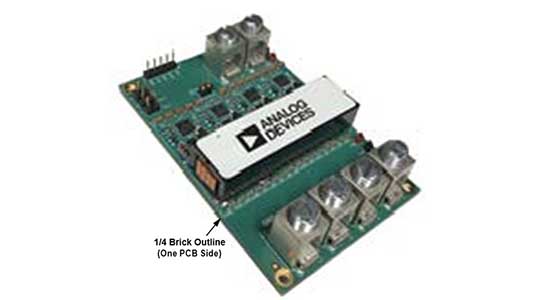
Designed CL = 4 × 1.1 μH is shown in Figure 4, replacing four DL = 6.8 μH inductors.5 Each DL is 28 mm × 28 mm × 16 mm, assuming that they are spaced 0.5 mm from each other: 4-phase CL with 56.5 mm × 18 mm × 12.6 mm dimensions achieves 4× volume reduction for magnetics. A complete 1.2 kW 48 V to 12 V regulated solution is shown in Figure 5, components on a single PCB side are inside 1/4-brick outline. The CL dimensions and footprint are purposefully designed to fit two CL parts inside an industry standard quarter-brick size. Placing all ~1 mm components (FETs, controller ICs, ceramic capacitors, etc.) on the bottom side of the PCB enables 1/8-brick size for the 1.2 kW solution.
Performance Gain
When the DL = 6.8 μH inductors were changed to CL = 4 × 1.1 μH—the current slew rate limit in the inductor also improved by 6×, which is always helpful for the transient improvement. On top of this, the inductor saturation rating improved by ~2× at 100°C, even though the total magnetics volume decreased by 4×.
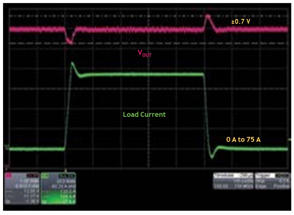
The transient performance of the proposed VIN = 48 V solution with the VO = 12 V output is illustrated in Figure 6. As expected, feedback regulates the output voltage to a preset value for the changing load current, also compensating for any changes in the input voltage.
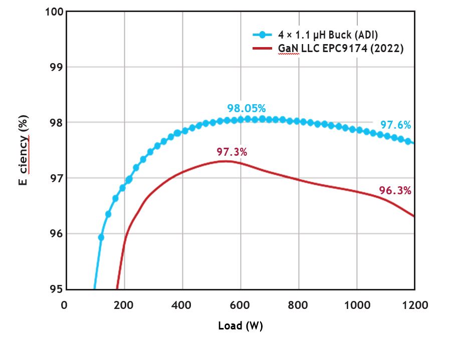
Probably the most important performance parameter, achieved efficiency is shown in Figure 7. It is compared to the state-of-the-art industry solution: 48 V to 12 V (fixed 4:1 step down) LLC with matrix transformer and GaN FETs on both primary and secondary sides.10 Compare the achieved full load efficiency of 97.6% and the benchmark of 96.3%. This implies that 16.6 W less losses are dissipated at full power, achieving 1.6× improvement in the proposed solution. Such loss reduction is typically very hard to achieve when the efficiency is already so high.
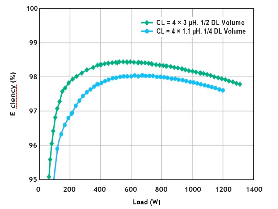
A trade-off between size and efficiency is certainly possible. Figure 8 compares the efficiency of the CL = 4 × 1.1 μH (4× reduction in magnetics size compared to DL) to a larger CL = 4 × 3 μH with only 2× reduction in inductor volume. The physically larger CL = 4 × 3 μH has a higher Lk = 3 μH value for leakage and a larger mutual inductance Lm = 10 μH. This allows a comfortable Fs reduction to 110 kHz, pushing the efficiency significantly higher in a whole load range.
Conclusion
Utilizing the coupled inductor benefits, the 48 V to 12 V solution reduces the total magnetics size by 4× from the base discrete inductors, achieving 1.2 kW in the industry standard 1/8 brick form factor. This 4× magnetics size reduction is achieved while preserving the excellent efficiency performance, increasing inductor current slew rate in transient by 6×, and increasing inductor Isat rating by 2×.
Compared to the industry state-of-the-art 48 V to 12 V solution in the same form factor: ~1.6× loss reduction is achieved at full power. Efficiency is also shown to improve further if a smaller reduction in magnetics size is acceptable.
At the same time, the proposed solution is fully regulated, placed directly on the customer motherboard, and utilizes standard silicon FETs to optimize the cost further. This is compared to unregulated 4:1 LLC with all GaN FETs, manufactured as a separate module with a specialized PCB that has many layers, a sensitive layout, and an embedded matrix transformer.
The overall performance gain illustrates the advantages of ADI’s patented IP on coupled inductors, which we are delighted to provide to our many customers with DC-to-DC applications.
References
- Aaron M. Schultz and Charles R. Sullivan. “Voltage Converter with Coupled Inductive Windings, and Associated Methods.” U.S. Patent 6,362,986, March 2001.
- Jieli Li. “Coupled Inductor Design in DC-DC Converters.” MS Thesis, 2001, Dartmouth College.
- Pit-Leong Wong, Peng Xu , P. Yang, and F. C. Lee. “Performance Improvements of Interleaving VRMs with Coupling Inductors.” IEEE Transactions on Power Electronics, Vol. 16, No. 4, July 2001.
- Yan Dong. “Investigation of Multiphase Coupled-Inductor Buck Converters in Point-of-Load Applications.” Ph.D. Thesis, 2009, Virginia Polytechnic Institute and State University, USA.
- Alexandr Ikriannikov. “Coupled Inductor with Improved Leakage Inductance Control.” U.S. Patent 8,102.233, January 2009.
- Alexandr Ikriannikov and Di Yao. “Addressing Core Loss in Coupled Inductors.” Electronic Design News, December 2016,
- Alexandr Ikriannikov. “Coupled Inductor Basics and Benefits.” Analog Devices, Inc., 2021.
- Alexandr Ikriannikov. “Evolution and Comparison of Magnetics for the Multiphase DC-DC Applications.” IEEE Applied Power Electronics Conference, March 2023.
- Alexandr Ikriannikov and Di Yao. “Converters with Multiphase Magnetics: TLVR vs CL and the Novel Optimized Structure.” PCIM Europe, May 2023.
- “EPC9174–Evaluation Board.” Efficient Power Conversion Corporation.
About the Authors
Alexandr Ikriannikov is a fellow for the Communications and Cloud Power Team at Analog Devices. He received his Ph.D. degree in electrical engineering from Caltech n 2000, where he studied power electronics from Dr. Cuk. His graduate school projects ranged from Power Factor Correction for AC-to-DC applications to 15 V to 400 V DC-to-DC for Mars rovers. After gradu- ate school he joined Power Ten to redesign and optimize multi-KW AC-to-DC power supplies, then in 2001 joined Volterra Semiconductor concentrating on low voltage high current applications and coupled inductors. Volterra was acquired by Maxim Integrated in 2013, which is now part of Analog Devices. Currently, Alexandr is a senior member of IEEE. He holds more than 60 issued U.S. patents plus more pending and has authored multiple publications in the field of power electronics.
Laszlo Lipcsei is a director for the Communications and Cloud Power Team at Analog Devices. He received his M.S.E.E. degree in automation and comput- ers from Bucharest Polytechnic University. In 2000, he joined O2Micro and focused on power conversion and battery management IC definition and development. In 2015, Laszlo joined Maxim Integrated AR&D team to lead the definition and system development of software-defined battery. His team also developed the wireless BMS proof of concept battery pack that was showcased at CES 2020. Since early 2020, he has been focusing on multi- phase and 48 V power conversion architecture development. Laszlo holds over 50 patents with more pending.


