Abstract
Assessing components for aerospace and defense applications can be inherently demanding due to strict requirements and system complexity. However, adhering to precise protocols can markedly reduce the chances of failures in the qualification phase. This article will present an overview of the Apollo MxFE AD9084, an Aadvanced wideband mixed-signal front end. During its qualification, a diverse set of protocols were implemented to ensure a flawless outcome. This article outlines some of the key procedures that were employed and how under- taking similar design approaches can help reduce risk.
Introduction
The conducting of a pretest or prescreening before qualification is very impor- tant to eliminate potentially weak components. Any devices that fail electrical tests should not proceed to further steps, which involve subjecting them to the qualification stress. One challenge arises when some units are near the test limits’ extremes. While they may initially pass the tests, these components might drift outside the limits during stress, leading to failures in the automated test equip- ment (ATE) results. Therefore, it is imperative to filter out these components that are close to the test limit outlier.
One approach is to perform an electrical test (etest) of the component before- hand using the production test limits, which offer three sigma protection from the actual test data limits. This constitutes the first round of testing. The second round of testing involves doing the pre-etest using qualification test limits that correspond to the data sheet limits without the guard bands.
This two-step screening process significantly reduces the likelihood of failures due to qualification stress. By eliminating components that are near the outliers, the risk of failure during the qualification stress phase is mitigated. This proactive approach enhances the overall reliability and performance of the components.
Useful Qualification Tools and Approaches
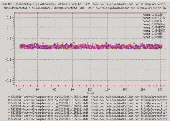
Figure 1 shows how statistical tools are used to ensure that the components pass pretesting and fall within the qualification specification limits (between upper and lower specification limits). It’s also crucial to assign a unique serial number to each unit during pretesting. For larger quantities, an electronic die ID is preferred for easy data comparison between pretest and posttest. A drift of less than 10% from the pretest limit is considered a pass, which requires invoking the electronic die ID during qualification testing.
To distinguish between device failure and test repeatability issues, a control unit is cycled through the same test sequence 50 times. If it passes all 50 times, it confirms test stability. However, if it fails after a few insertions, it suggests a test repeatability issue, warranting further investigation. Analyzing poststress data helps identify potential test-related problems. If found, the test program needs optimization, rather than labeling it as a device failure.
For complex devices like Analog Devices’ Apollo MxFE AD9084, it’s vital to run con- trol units even during high temperature stress testing. Given that it runs at 37 W, separate control units can safeguard against potential power supply issues.
Another common mode of device failure is voltage transients during power rail switching. When the power rail is switched on there may be power glitches in the first few milliseconds that may damage the device. If there is a power interrup- tion in the reliability lab and if the power generator is to be turned on, there are chances voltage transients may occur, which may in turn damage the device. This is known as electrical overstress (EOS). However, to prevent this mechanism, one of the simpler procedures is to add a transient voltage suppression (TVS) diode. The TVS diode is added as a shunt in the power supply path. If a voltage tran- sient occurs, the TVS diode activates first, preventing EOS damage and effectively reducing device failure during qualification.
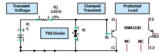
Figure 2 shows a TVS diode in action, preventing a power glitch and adverse effects on the component. Prevention such as this can help avoid requalifica- tion, schedule delays, and spending of extra resources. In the development of the Apollo MxFE AD9084, preventing these factors were key design considerations.
During qualification, another type of failure that can occur is related to moisture sensitivity levels (MSL) stress. This stress is typically preceded by a confocal scan- ning acoustic microscopy (CSAM) study during the reflow and bake process. MSL is also referred to as a package level qualification stress. Sometimes, CSAM images reveal die delamination after the stress and post-etest phase. CSAM is a quick, nondestructive analysis technique that uses ultrasound waves to detect changes in acoustic properties within integrated circuits and similar materials.
According to the JEDEC standard, if the die delamination between the epoxy and die exceeds 10%, it is considered a failure. One way to prevent this is to perform a CSAM and thru-scan analysis during the qualification process. Thru-scan, also nown as acoustic microscopy in transmission mode, is particularly effective at detecting delamination at the die-attach interface.
To further prevent die delamination, it’s important to consider two factors. First, check the epoxy and curing profile temperatures to ensure they are within the appropriate range. Second, during the assembly process, especially if a high pressure wash was involved, confirm that it effectively removed all flux residue. Additionally, selecting the correct MSL level is crucial. For laminate-based pack- ages, targeting MSL 3 is advisable. Using MSL levels 1 or 2 can lead to failures.
For larger electronic packages such as a 10 mm2 × 10 mm2 thin quad flat package (TQFP), opting for an MSL level of 3 is preferable over MSL 1 to reduce the risk of die delamination and potential device failure.
Helpful Qualification Tests
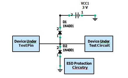
A leakage test is an important pre-etest sequencer that can help to determine if there is a process defectivity. A leakage test involves powering down the device and applying both positive and zero voltage to check for any current flow. If cur- rent is detected, it indicates a process defect, and those units should not undergo qualification stress. Subjecting them to stress might lead to a false failure, mak- ing it challenging to identify the root cause, which could be related to the fabrica- tion process.
However, incorporating hardware for a leakage test into the final hardware inter- face board (HIB) can be complex. To address this, a probe card can be constructed to conduct the leakage test even before the die is assembled into the final pack- age. This enables early identification of any process defects.
Another common failure during qualification arises from assembly issues. This can be attributed to factors such as Copper pillar on silicon or high pin-count BGA packages, which can reach up to 900 pins, sometimes leading to complications with under-bump metallurgy. One effective way to identify and address assembly issues is by implementing a continuity test, encompassing both positive and neg- ative continuity testing. This enables the early detection of assembly problems, even before the functional and parametric tests are conducted. It also aids in pin- pointing the source of the issue. In some cases, continuity testing is conducted at the die level using a probe card prior to the final package assembly. This practice not only reduces costs but also provides an estimate of final sample quantities, contributing to cost reduction and better planning for the team.
It’s important to note that a continuity test indicates an assembly-related issue, which is distinct from a device-related qualification failure. If a failure is related to the packaging process, it is considered a packaging-related issue in terms of qualification. However, if it’s an issue related to packaging, steps can be taken to rectify it. One common area for assembly issues is wire bonder misalignment, epoxy application, and curing profile temperature. It has been observed that a significant portion of reliability failures over the years can be attributed to assem- bly-related issues. Therefore, implementing a robust approach to electronic pack- aging during assembly can significantly reduce qualification-related failures.
The direct current high temperature operating life (DCHTOL) test is crucial for pre- dicting device reliability over time. By stressing the device from 70°C to 125°C, we find an acceleration factor (AF) of about 118. This means that each hour of testing at 125°C is equivalent to roughly 118 hours of normal use at 70°C.
For 1,000 hours of DCHTOL stress, it translates to approximately 13.58 years. This stress is especially critical for ADI’s Apollo MxFE AD9084, used in phased array radars and space applications, where devices are expected to operate for significant time periods.

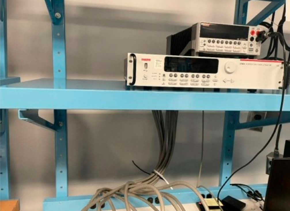
During testing, issues like loading or heat sink problems can be prevented by monitoring the I/V curve. This helps catch any problems early, avoiding false fail- ures during qualification.
Another way to prevent qualification failures is by conducting additional tests before sending a failed unit for analysis. One effective test is measuring contact resistance. This helps pinpoint the location and cause of the failure.
High temperature operating life (HTOL) testing is another critical phase where devices can fail. Properly determining thermal resistance (theta Jc) is vital to avoid overheating. Thermal scans provide crucial insights, helping identify over- heating areas and allowing corrective actions.
Electrostatic discharge (ESD) can also lead to failures during qualification. Including control units in testing alongside units undergoing ESD helps ensure adherence to ESD protocols, confirming proper handling during the process.
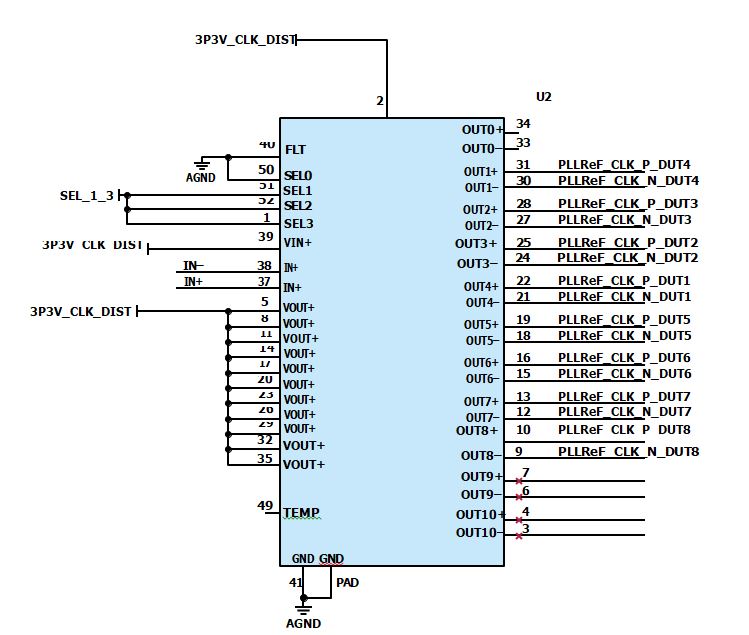
Grouping pins based on function and applying ESD in separate compartments reduces the risk of ESD failures. Additionally, for sophisticated devices like the Apollo MxFE, careful clock conditioning is essential, especially when using inter- nal PLLs or clocks. Proper oscillator frequency and voltage levels are critical to ensure reliable testing. Addressing issues with crystal oscillator circuitry during HTOL testing is important. Modifying the schematic and layout helps, but implementing these changes in the qualification board may entail significant costs. To avoid this, an adaptor board policy such as that adopted by ADI’s AD9084 can be a cost-effective solution.
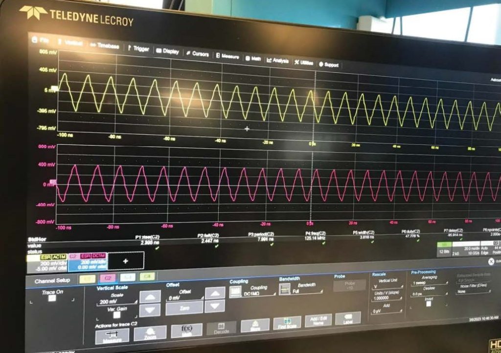
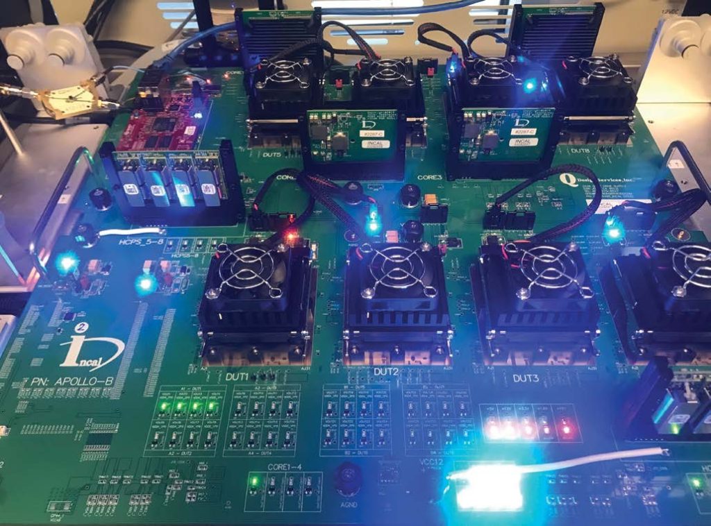
As depicted in the example of ADI’s Apollo MxFE shown in Figure 6, each of the adaptor boards with the modified clocking scheme underwent individual verifica- tion. The subsequent challenge was to affix these adaptor boards onto the existing HTOL boards, which had a flawed clocking scheme. The specific solder points were identified, and the adaptor boards were successfully soldered onto the existing HTOL board. This adaptation worked seamlessly, resulting in substantial cost and time savings that would’ve been spent on redeveloping a new board. Following the optimization of the clocking scheme and the completion of the qualification for the AD9084, no failures were observed during any HTOL tests undertaken to date.
Adhering to the guidelines outlined in this article can effectively diminish the occurrence of qualification failures. It’s important to note that a significant por- tion of these failures is attributed to external factors rather than inherent issues with a component. However, by diligently following these steps, not only can the incidence of qualification setbacks be lowered but also a thorough analysis to pinpoint the root causes can be conducted. This streamlined approach aids in timely product release to the market, while also minimizing the requirement for testers and man-hours. Additionally, it facilitates the identification of specific areas of concern, allowing for comprehensive feedback to be provided to the design team.
Conclusion
ADI is committed to delivering reliable, high performance solutions and continually enhancing internal processes to achieve this goal. Since the qualification of the Apollo MxFE, additional qualification tests and processes have been introduced. These enhancements encompass various aspects, including current and voltage measurements for individual devices under stress (DUST). Comparators are also being used to monitor whether the voltage surpasses the target value, with LED indicators signaling the status. Furthermore, to bolster reliability, a watchdog timer controlled by a microcontroller has been incorporated to serve as a safeguard and shut the system down in the event of a power glitch, preventing any potential dam- age to the reliability units. Improvements such as these help to further ensure zero failures during the qualification of highly complex integrated circuits.
About the Author
Rajesh Sur is a staff product engineer with Analog Devices. He earned a B.S.E.E. degree from MIT Manipal, an M.S.E.E. from University of Arkansas, Fayetteville, and an M.B.A. degree from Wake Forest University. Rajesh is a senior member of the IEEE. He currently holds 521 worldwide patents including more than 100 U.S. patent grants. He is the author of four techni- cal books. Rajesh has 23 years’ experience as a senior product engineer, senior packaging engineer, and product engineering manager having pre- viously worked at Texas Instruments, Freescale Semiconductor, and Qorvo.


