Abstract
This article aims to demonstrate that even controller-based products with discrete power switches and catch diodes can achieve low emissions. It will delve into the significance of good PCB layout and controlled switch edge rates in meeting low emissions standards. Additionally, it presents two reference designs that successfully pass CISPR 25 Class 5 emissions testing.
Introduction
The goal of many automotive and industrial applications is to reduce emissions in switch-mode power supplies (SMPS). SMPS have gained a reputation for being noisy and challenging to meet CISPR emissions standards. Efforts to enhance low emissions in SMPS have been ongoing for the past decade, culminating in the development of one of the first nonsynchronous boost controller ICs (external power switch) that focuses on significantly reducing electromagnetic interfer- ence (EMI) with ease.
Monolithic switchers are highly convenient for use in DC-to-DC converter applica- tions. They require minimal external components due to the integration of power components, control loops, and other functions. While integrating power switches simplifies board design and layout, it comes with the trade-off of reduced out- put power when external power switches are not used. The compact hot-loop and reduced emissions of the integrated switches concentrate all the high power losses within the limited space of the IC package. This can pose thermal performance challenges, particularly in high power, high frequency, or high volt- age systems. Many applications require power levels beyond what a monolithic can provide, reaching up to 50 W. Therefore, there is still a demand for controller ICs that drive external power FETs.
To meet the growing need for boost converters with low emissions, a new boost controller has been developed. This nonsynchronous controller is capable of driv- ing a single, high voltage power switch, offering versatility as both a boost and single-ended primary inductor converter (SEPIC). Automotive applications, in particular, require a wide input voltage range, low quiescent current, and spread spectrum features. The LT8357 provides a simple, compact, and efficient solution for industrial, automotive, and battery-powered systems (see Figure 1).
Analog Devices has made significant efforts in recent years to push the boundar- ies of low emissions in switching converters. The introduction of Silent Switcher® technology has become synonymous with achieving the best emissions pos-
sible. In 2020, the first Silent Switcher monolithic boost converter, the LT8336, was released. Silent Switcher ICs are monolithic converters that integrate syn- chronous power switches. These ICs incorporate various techniques to minimize emissions caused by switching hot loops, including the integration or reduction of hot loops.1
While Silent Switcher architecture is one approach to achieving low emissions, it is not the only method. Monolithic nonsynchronous converters, which integrate only one power switch into the IC silicon or package, can also achieve low emissions.2
Layout Is Important!
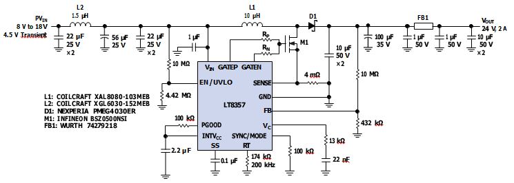
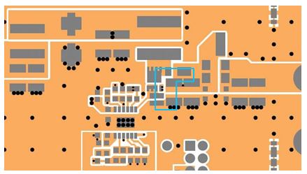
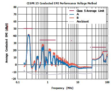
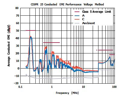
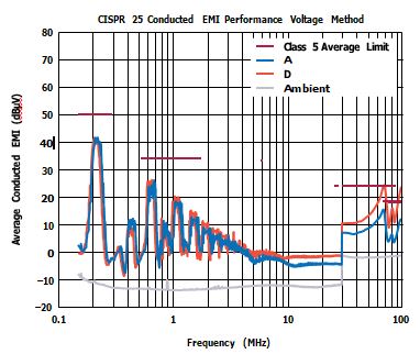
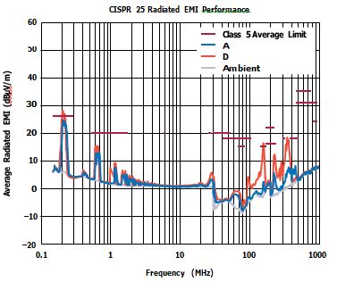
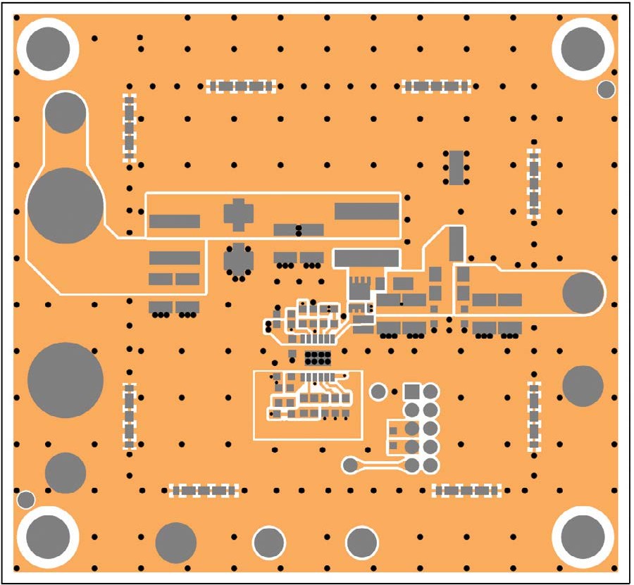
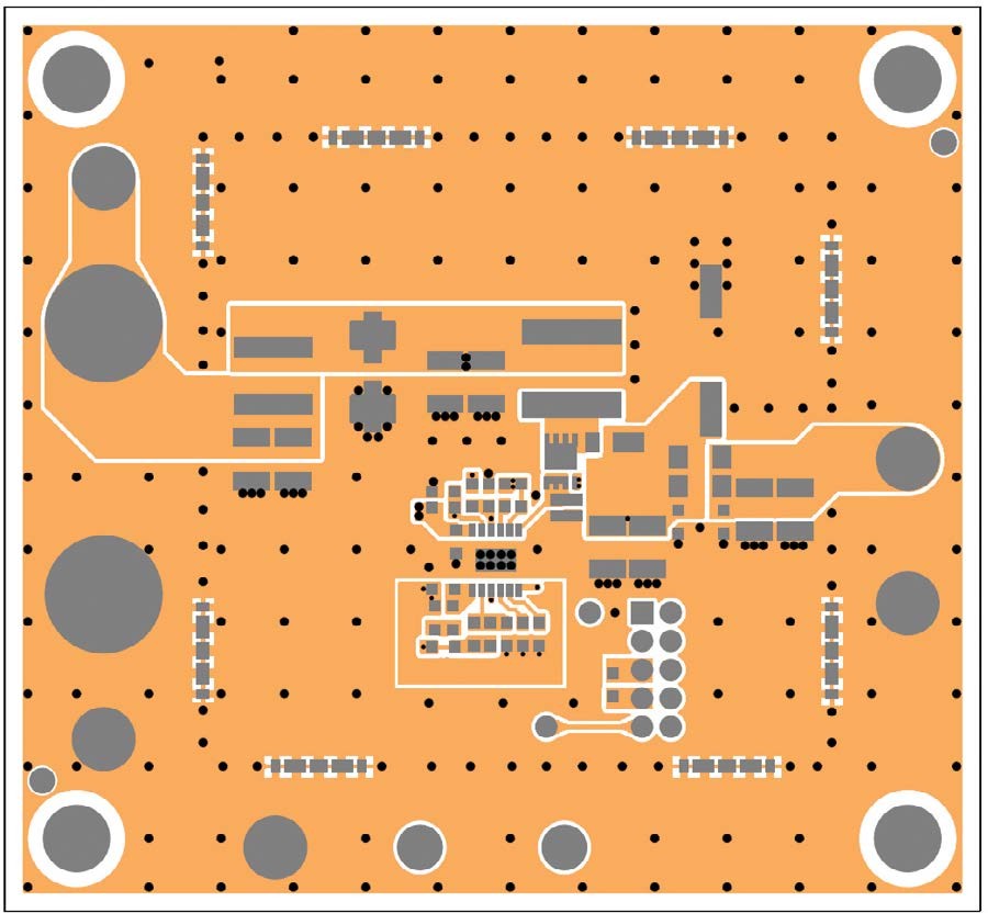
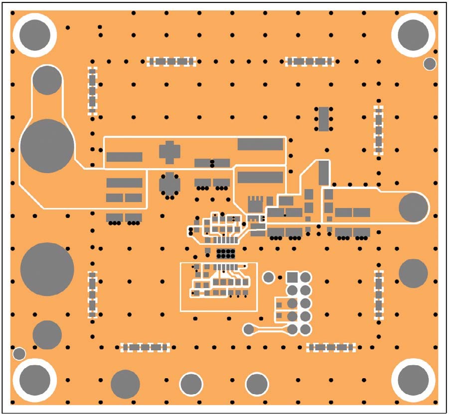
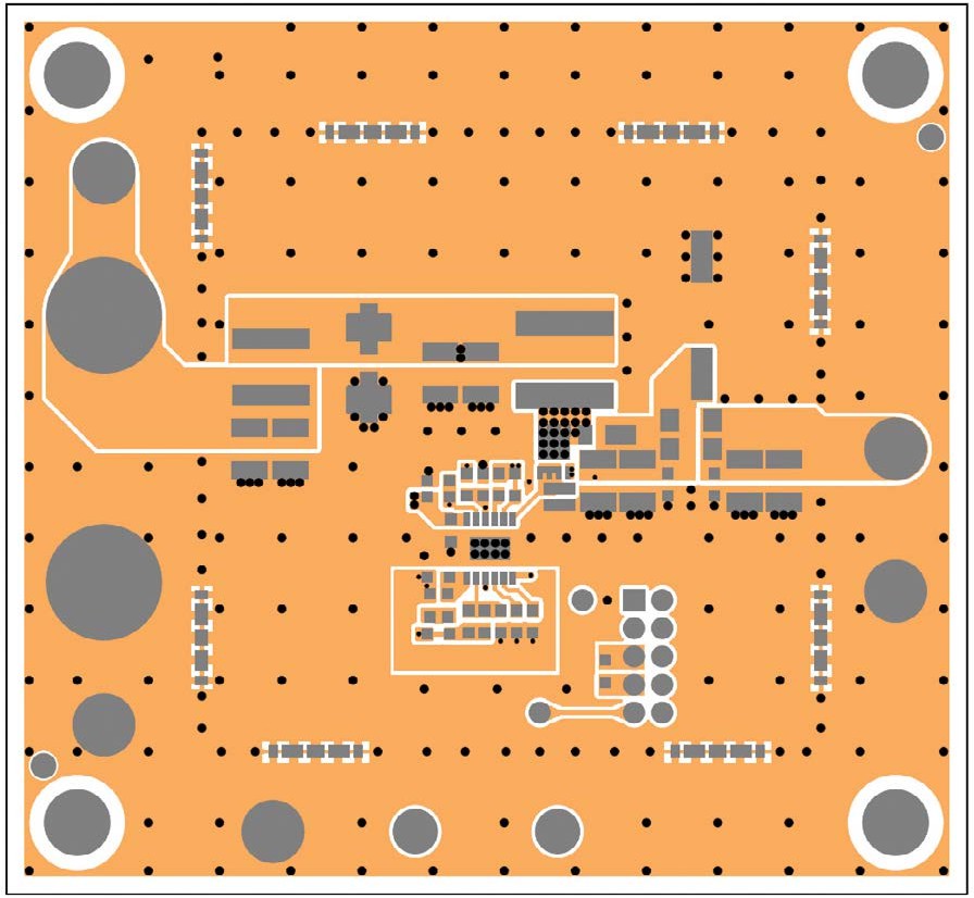
One crucial aspect of achieving low emissions in SMPS converters, particularly with controller ICs, is careful attention to PCB layout. Unlike monolithic solutions that offer switch integration to aid with emissions, controller ICs require additional considerations for minimizing emissions and meeting CISPR standards. The article provides tips to maximize performance, with Figure 7 offering guidance on the best layout for emissions, while Figure 8 to Figure 10 demonstrate modified layouts using poor techniques.
Hot Loop Management
Nonsynchronous switch-mode boost converters require the use of a main switch and an output catch diode. In contrast, synchronous converters use two gate driv- ers and power switches that are synchronized by the control logic to minimize potential catch-diode (nonsynchronous) conduction losses. However, synchronous converters introduce complexities such as gate-timing requirements to prevent shoot-through currents, and the need for additional silicon space (and cost) for high-side gate drivers. Nonsynchronous converters only require a single gate driver and do not need the blanking time between the power switch and catch diode.
However, the high current switching action between these two components can pose challenges in low EMI converters. To mitigate potential issues, it is consid- ered best practice to minimize the hot loop in a boost converter. The hot loop consists of three components: the main switch, catch diode (or synchronous switch), and output capacitor. Typically (as is the case in the LT8357), the peak switch current sense resistor is also part of the hot loop (see Figure 2). In a SEPIC configuration, the coupling capacitor between the two windings is also included in the hot loop. Having large hot loops introduces additional trace inductance in the high current switching paths. This extra inductance can lead to voltage spikes on the respective nodes, unfortunately becoming a significant source of emissions. Figure 3 shows how hot loop management helps reduce some emissions in the conducted voltage test.
Shrink the Switch Node Plane
Reducing the size of the switch node plane is another important consideration in the development of low EMI boards. The switch node plane consists of the switch’s drain, one leg of the inductor, and the anode of the catch diode. While it may be tempting to have a large switch node plane to increase the surface area for thermal conduction, this can lead to increased emissions. Figure 4 shows how shrinking the switch node plane can help reduce conducted voltage emissions in specific areas.
Keep the Switch Node Plane on One Layer
It is crucial to keep the switch node plane on a single layer whenever possible. In some cases, designers may be tempted to place the inductor on one side, and the switch on the other due to size limitations. However, this requires the switch node plane to pass through some vias, traverse to another layer, and then come back up again. While this approach may save board space, it results in increased emissions. The vias on the switch node can act as additional antennas, emitting noise and other radiation that can be easily detected by the antennas used for measuring emissions. Figures 5 and 6 detail the emissions generated by vias on the switch node.
Switch Frequency Up to 2 MHz with Spread Spectrum Frequency Modulation (SSFM)
As devices continue to shrink and pack more functionality and power requirements into smaller areas, there is a growing need to reduce board area, starting with the power supply. The inductor, typically the largest component, poses a challenge in achieving board area reduction. It is well-documented that in switching convert- ers, the required inductance is inversely proportional to the switching frequency. For example, if a design requires a 10 μH inductor for 200 kHz, the same power requirements at 2 MHz would only require a 1 μH inductor. The LT8357 offers the flexibility of switching frequencies up to 2 MHz, allowing for significant reduction in inductor size and consequently shrinking the switch node. This reduction in size can potentially benefit emissions.
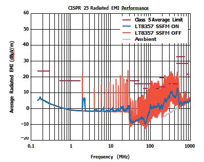
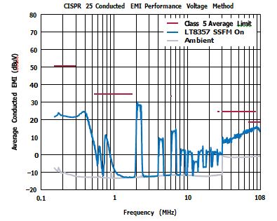
Switching at 2 MHz also brings another important advantage. CISPR 25 imposes a limit from 530 kHz to 1.8 MHz, known as the MW band, which contains the AM radio band. To comply with regulations, it is recommended to avoid setting the switch- ing frequency within this range. By switching at 2 MHz, this band is completely avoided, providing some margin for compliance. The fundamental frequency of the emissions plot aligns precisely at 2 MHz, with subsequent harmonic falling at higher frequencies. This eliminates the need for a bulky low frequency filter to attenuate emissions below the lower frequency CISPR limits. In some cases, despite efforts, the fundamental frequency and harmonics may still exceed the limits. To address this, ADI introduces the first boost controller to feature SSFM. This feature is paramount for passing CISPR 25 emissions stan- dards. The IC intelligently spreads the switching frequency up to 19% above the set frequency using a triangular spread. This spreading technique helps reduce emissions peaking at the minimum and maximum frequencies. Figure 11 shows how the built-in SSFM function affects the emissions spectrum, aiding in emis- sions reduction to meet the CISPR standards.

Split Gate Driver and Switch Node Edge Rate Control
During each cycle, the switch node undergoes a transition (rises and falls) from 0 V to VOUT, which is responsible for a significant portion of high frequency emis- sions. In monolithic converters, the IC design determines the switch node rise and fall characteristics, and users have no control over this aspect. Fortunately, many monolithic converters are designed to minimize emissions by controlling the switch edge behavior.
For controllers, the switch is external, and the controller provides a gate driving signal to control the external switch. A good controller has precise control over the switch turn-on to effectively manage the rise and fall of the switch’s drain. Proper control of the switch’s rise and fall results in a substantial reduction in high frequency radiated emissions. Additionally, using a gate resistor (typically around 5 Ω) can further decrease radiated emissions at high frequencies, although it comes at the cost of lower efficiency. This trade-off introduces additional switch- ing losses due to slower turn-on and turn-off times.
The LT8357 introduces a unique split gate driver feature. Previously, a user could only control both the gate turn-on and turn-off with a single resistor. The new split gate driver allows for precise and independent control over the gate’s turn-on and turn-off. Through experimentation, it has been found that the gate turn-on con- tributes significantly more to radiated emissions than the turn-off. Having precise control over which edge to slow down provides a significant advantage. By inserting a gate resistor for the pull-up, and omitting it for the pull-down, emissions can be minimized while maintaining high efficiency.
Edge Rate and Switching Emissions
Figure 12 shows the EVAL-LT8357-AZ emissions comparison between different gate resistors. According to Figure 12, the gate resistors primarily affect emis- sions in the 400 MHz to 500 MHz range.
It is observed that the pull-up resistor has a more significant impact on emissions reductions compared to the pull-down resistor, which has a minimal effect. Therefore, for optimal power loss savings and emissions reduction, it is recom- mended to use a small 5 Ω resistor as the pull-up resistor and no resistance or a short for the pull-down resistor.
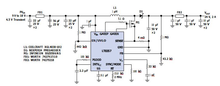
For example, the EVAL-LT8357-AZ utilizes a 5.1 Ω pull-up resistor, and no pulldown resistor.
Power Loss Savings
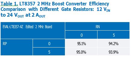
Table 1 shows differences in the efficiency of the 2 MHz, 12 V input to 24 V, 2 A output boost converter with shorted input and output EMI filters. According to the data, the best power savings are achieved by reducing the RN resistor to 0 Ω. Switching power loss equations are as follows:
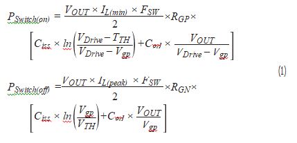
RGP is the combination of the device’s “Gate Pull-up Resistance” from the data sheet, user-selected pull-up gate resistor, and gate resistance RG from the switch data sheet. RGN is the combination of all the same, but with pull-down resistances. Ciss, Cgd, Vgp, and VTH can all be found in the power switch’s data sheet.
The resistance between the gate driver and switch gate directly affects power loss. When all the calculations are performed, it is evident that the turn-off switching loss is quite significant. Interestingly, the equation for switch off powerloss yields higher losses with the same gate resistance due to the higher current flowing through the switch during turn-off. Since the gate turn-off does not contribute significantly to emissions, using a 0 Ω resistor (or short) from the GATEN pin to the switch gate optimizes efficiency and emissions. For example, a 2 MHz switching converter can achieve a few percentage points of efficiency improve- ment simply by eliminating the pull-down gate resistor. This improvement should not be underestimated. The split gate resistor offers the benefits of emissions reduction without sacrificing the efficiency associated with extra gate resistors.
EVAL-LT8357-AZ 2MHz Modification
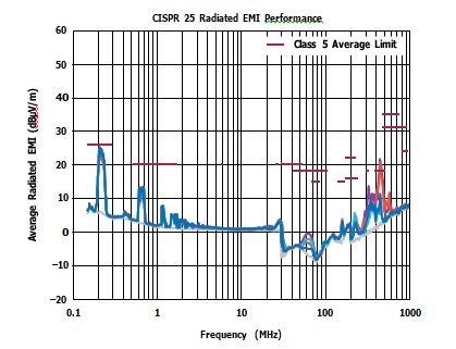
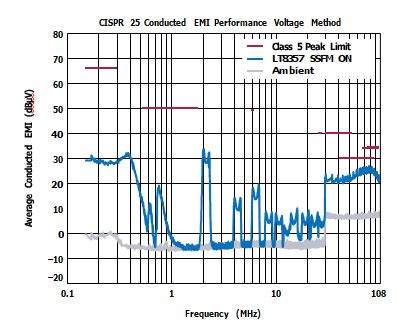
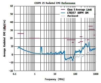
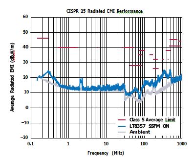
The EVAL-LT8357-AZ is a boost converter designed for low EMI at a switching fre- quency of 200 kHz. It is equipped with a relatively large 8 mm × 8 mm × 8 mm inductor. However, if a user finds the inductor size to be too large, the board can be easily modified to operate at a 2 MHz switching frequency while maintaining the same voltage and power specifications. This modification allows for a significant reduction in the size of the inductor, which can shrink from 8 mm × 8 mm × 8 mm to a smaller 4 mm × 4 mm, 3 mm tall XGL4030-102 inductor. Additionally, the need for the bulk hybrid polymer output capacitor is eliminated, and the input EMI filter can be made smaller. These modifications result in substantial board space savings, while still enabling operation from a 12 V input source to 24 V, 2 A output. Figures 15 to 18 show the 2 MHz board under CISPR 25 Class 5 emissions standards.
Conclusion
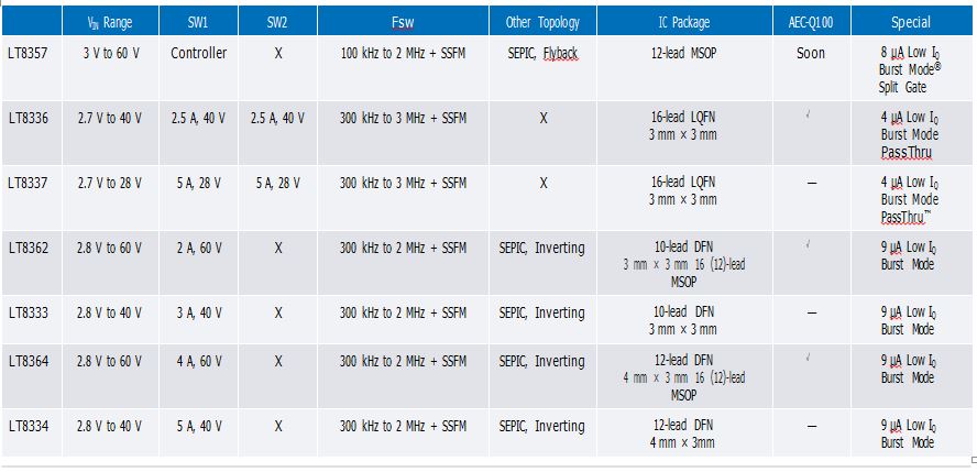
The LT8357 boost controller is a feature-rich product designed for low emis- sions, yet it remains user friendly. The 10 lead IC is neither overly complex nor too simplistic to design around. It does not include unnecessary features like a synchronous switch, ensuring a streamlined design. There are a sufficient number of features to maintain high efficiency and low emissions. The combination of features, along with the ease of design allows the device to be a perfect addition to the low emissions boost converter family shown in Table 2.
This new generation boost controller is specifically designed to meet the growing demand for high voltage and high current boost converters with low emissions. It is a nonsynchronous controller that drives a single, high voltage power switch, providing versatility as both a boost and SEPIC converter. Furthermore, the cus- tomizability extends beyond this point. Its current mode architecture allows for adjustable and synchronizable fixed frequency operation from 100 kHz to 2 MHz. An internal 19% triangle SSFM operation can be enabled or disabled, resulting in improved EMI performance. The split 5 V gate driver is a valuable tool for optimiz- ing the trade-off between emissions and efficiency in an N-channel MOSFET or GaNFET. With a wide 3 V to 60 V input voltage range, dedicated PGOOD pin, and a low quiescent current of 8 μA, the boost controller provides a simple, compact, and efficient solution for industrial, automotive, and battery-powered systems.
References
1 Tony Armstrong. “Silent Switcher Devices Are Quiet and Simple.” Analog Dialogue, Vol. 53, April 2019.
2 Keith Szolusha and Kevin Thai. “Can Nonsynchronous DC-to-DC Boost Converters
(with a Catch Diode) Still Have Low Emissions?” Analog Devices, Inc., March 2022.
“Power MOSFET Basics: Understanding Gate Charge and Using It to Assess Switching Performance.” Vishay, February 2016.
“How to Select the Right CoolMOS and Its Power Handling Capability.” Infineon Technologies, 2002.
BSZ0500NSI. Infineon Technologies, 2021. BSZ0506NS. Infineon Technologies, 2021.
Lakkas, George. “MOSFET Power Losses and How They Affect Power-Supply Efficiency.” Texas Instruments, 2015.
About the Authors
Kevin Thai is an applications manager with Analog Devices in San Jose, California. He works in the IPS Power Products Group and oversees the isolated flyback and protection product lines along with other boost, buck-boost, and GaN controller products. He received his B.S. degree in electrical engineering from Cal Poly, San Luis Obispo, in 2017, and M.S. degree in electrical engineering from University of California, Los Angeles, in 2018.
Keith Szolusha is an applications director with Analog Devices in San Jose, California. Keith has worked in the IPS Power Products Group since 2000, focusing on buck, boost, buck-boost, LED, and GaN controller and driver products, while also managing the power products EMI chamber. He received his B.S.E.E. degree in 1997 and M.S.E.E degree in 1998 from MIT in Cambridge, Massachusetts, with a concentration in technical writing.


