The market for advanced driver assistance systems (ADAS) is one of the fastest growing for automotive electronics. Cameras are a key element of the ADAS sensors toolset (Figure 1). Installed in selected locations around the vehicle exterior, an increasing number of cameras are used to deliver a surround view experience, giving drivers new and previously unobtainable exterior views. The numerous benefits range from monitoring blindspots when changing lanes on the highway and aiding with parallel parking, to automatic traffic sign recognition and pedestrian detection. Advanced cruise control and situation-aware collision-avoidance systems are on the horizon. These remote camera modules, with their on-board power management systems, must be small, efficient, and cost-effective.
This article discusses the shortcomings posed by a typical automotive remote camera power management implementation, and presents a highly integrated solution that occupies a fraction of the PC board (PCB) space while preserving high levels of efficiency.

Powering the Remote Camera
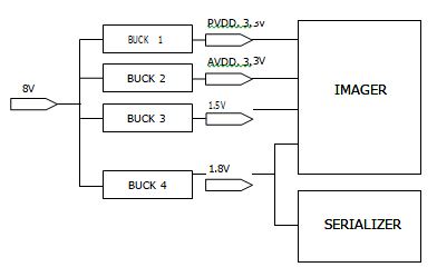
The remote camera module is typically powered by a power- over-coax (POC) 8V rail and consumes approximately 1W or less (< 125mA). This rail is bucked down to power the on-board electronic loads, including the imager and the serializer (Figure 2). The camera operates in an on/off fashion; either on at full operation or completely off. For this reason, it is more cost- effective to select streamlined buck converter ICs designed for high efficiency at full load without extra silicon (or costs) devoted to enhancing light-load operation. In Figure 2, the passive components are omitted for simplicity.
The Typical Solution: Discrete Bucks
The typical solution implements each rail with a dedicated, 8V-powered, discrete buck converter. The four converters are usually designed around identical ICs, for economies of scale and ease of design. However, since the buck converter loads are quite different, the overall design is inherently inefficient.
Reduced Efficiency
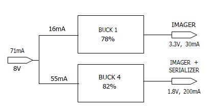
In this section, only two of the four rails (Buck 1 and Buck 4) are discussed in detail. Buck 2 and Buck 3 mirror the situation of Buck 1 and Buck 4, and are not discussed for brevity.
The efficiency of Buck 1 with a 30mA load is suboptimal (78%) since it operates under a light load. The efficiency of Buck 4 is also suboptimal (82%) since it operates at a low duty cycle (1.8V/8V = 0.225). The net result is a system draw of 71mA from the 8V rail (568mW).
High Cost and Large Footprint
This discrete solution is costly and space-consuming, requiring one IC for each rail and the related passive components. As shown in Figure 4, the PCB space required by two of the four buck converters, including passives, is 160.4mm2.
A Superior Solution: Dual Buck
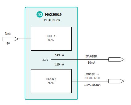
By covering the four rails with two dual-buck converter ICs, we save additional space and preserve efficiency. Figure 5 shows the dual-buck solution for two of the four rails using the MAX20019. External passive components are omitted for simplicity.
Efficiency Preservation
With the MAX20019, two integrated buck converters are optimized for cascaded operation, both working at or near full load and high duty cycle for the highest efficiency. The 1.8V buck converter, with only 3.3V at its input (as opposed to 8V in the typical architecture), is optimized for a mid-range duty cycle (1.8V/3.3V = 0.545), and operates at a 92% peak efficiency. The 3.3V buck converter is optimized for duty cycles from POC voltages of 8V (3.3V/8V = 0.412) to 12V and at near-full load, yielding a respectable 86% efficiency with 8V input. The net result is a draw of 71mA from the 8V rail, which demonstrates how this configuration preserves efficiency. More importantly, this solution reduces the bill of materials by using a single IC and smaller passives (more on this in the next section).
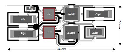
Many enhancements contribute to the dual-buck solution size advantage. First, the integration of two buck converters into a single chip helps reduce the PCB footprint by eliminating one IC package. Second, the high clock frequency (3.2MHz) and fast transient response further reduce the PCB footprint by minimizing the sizes of the output inductors and capacitors. Third, out-of-phase clocks between the two converters smooth out the input current, reducing the size of the input capacitors. Figure 6 illustrates the PCB footprint with the MAX20019.
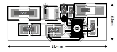
The integrated dual-buck solution occupies a PCB area of only 125.1mm2 resulting in a whopping 22% PCB area reduction.
A second MAX20019 can be used for the other two rails depicted in Figure 2 (Buck 2 and Buck 3). The entire remote camera POC is efficiently provided with only two ICs and their related passives.
Low Noise Solution
An additional advantage of the MAX20019 is the internally fixed frequency at 3.2MHz, which allows for small external components, reduced output ripple, and operation above the AM band to reduce radio frequency interference. The device operates at constant frequency in forced PWM mode (FPWM) and offers optional spread-spectrum frequency modulation to minimize EMI-radiated emissions due to the modulation frequency.
Remote Camera Module
Figure 7 shows the Maxim Integrated remote camera module PCB prototype with two MAX20019 ICs implementing the POC solution for the four power rails.
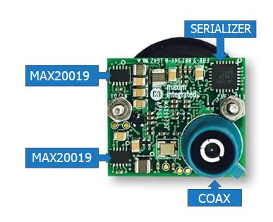
The compact 870mil x 750mil PCB demonstrates the MAX20019’s ability to support a state-of-the art, miniature, and power-efficient remote camera solution.
Conclusion
Remote camera modules, which include on-board power management systems, must be small, efficient, and cost- effective. Typical power management solutions are space and power inefficient since they utilize multiple ICs and operate with suboptimal efficiency. The MAX20019 dual-buck converter, optimized for cascaded operation, enables remote camera power management solutions that occupy a fraction of the typical PCB space while preserving high levels of efficiency.
Learn More : MAX20019 3.2MHz, 500mA Dual Step-Down Converter for Automotive Cameras


