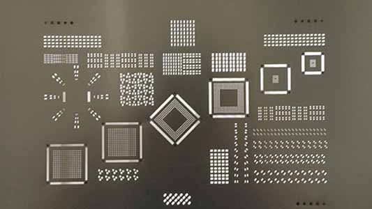
Due to its economic advantages over traditionally costly evaporation and electroplating processes Stencil printing remains the technology route of choice for flip chip bumping. This Article brings up all the technological challenges and latest advancements in all processing steps of 6”wafer bumping of peripheral array structures at Ultra-fine-pitches (UFP) of 100µm pitch and especially 60µm pitch. Innovative electroformed stencils have been manufactured with a thickness down to 20µm. Both type 7 (2-11µm) and type 6 (5-15µm) pastes of eutectic composition Sn63/Pb37 have been successfully employed for wafer bumping at 100µm pitch. Bumping using 25 µm stencil thickness has yielded bump heights of 42.3±3.8µm and 43.6±3.5µm for type 7 and type 6 pastes, respectively. A newly developed type 8 paste (2-8µm) has been used for the first time to bump chips with peripheral contacts at 60µm pitch. A 20µm thick electroformed stencil was used with 35µmx80 µm oblong apertures. Printing at 60µm pitch has yielded very promising results and has proved the capability of electroformed technology to manufacture accurate and robust thin stencils. The bump height at 60µm pitch was measured to be 28 ±3 µm.
Introduction
Stencil printing is a process of placing solder paste on the printed wiring boards (PWBs) in order to establish electrical connections. The equipment used in this process are stencil, solder paste, and printer. The stencil printer is also popularly known as a screen printer. Stencil is a thick paper with designs punched with letters. As a print medium, ink is run through the paper to imprint the letters correctly. Stencils are used to cut designs or letters and later allow the pigment medium, which in either case could be ink, solder paste, or at times, electrical current on to the PWBs through the cut-out holes.

The attractiveness of flip chip technologies lays on the superior electrical performance, higher thermal conductivity, smaller size and higher I/O counts which are mandatory requirements for advanced semiconductor applications. However, a substantive shift towards flip chip interconnection technologies will be witnessed only with accomplishment of cost reduction, reliability improvement and cost-efficient high density substrate technologies. Low-cost flip chip bumping technology has become a reality with implementation of electroless nickel plating process for under bump metallization (UBM) in conjunction with stencil printing of solder pastes for the formation of solder bumps
Stencil printing of solder paste for flip chip wafer bumping offers among others the advantages of cost- effectiveness and compatibility with pre-existing printing equipment in a surface mount assembly line. The state-of-the-art in wafer bumping using the conventional stencil printing technology (laser- cut steel and Nickel-electroformed stencils) is at about 120µm pitch for peripheral arrays and 150µm for area arrays. This progress is extremely significant especially in view of Moore’s law prediction that the bits/chip grow by a factor of 4x every three years. However, the advancements to UFP bumping cannot be realized without parallel progression to very fine paste and stencil manufacturing. The emergence of ultra fine type 7 pastes (2-11µm) and lately of type 8 (2-8µm) pastes as well as recent developments in fabrication of very thin electroformed stencils with very small aperture dimensions have sparked significant work in the area of UFP wafer bumping.
Stencil design rules & Selection of stencil manufacturing method
The criteria for the selection of stencil manufacturing technology were aperture wall quality, dimensional consistency, positional accuracy and stencil production cost. Recent refinements in the laser cutting process have been developed to improve even more the quality of stencil apertures including smaller laser spot sizes and water guided laser cutting techniques. One advantage of laser cut stencils compared to electroform is that the material is pre-tensioned from the framing process prior to cutting, which in turn reduces the stencil deformation. Laser cutting is a sequential process; therefore as the number of I/O increase on the design so does the time to manufacture the stencil. This can be a significant disadvantage for wafer bumping stencils at fine and ultra fine (<120µm) pitches with a high number of apertures because as the number of holes increases the manufacturing time rises to an almost uneconomical point. Also the heat melt interaction during the cutting process can create rough inner sidewalls which in turn produce apertures with a larger surface area and therefore have a tendency to minimize paste release. In addition, the heat generated in the cutting process must be controlled as not to warp the stencil during manufacturing or damage the fine webs required for UFP printing. Electro polished stencils are normally laser cut stencils which have been smoothed using electrochemical or mechanical polishing methods. However all metal stencil types can be treated in this manner after manufacturing.
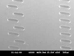
Stencil thickness: 20µm
The cost factor becomes profoundly significant considering an approximate cost of 3 $/100 laser-cut apertures and the large number of apertures needed for UFP structures. In contrast, electroformed stencils with good aperture wall quality and reasonable manufacturing cost per wafer design; and not per aperture, appear as a rational alternative solution especially for UFP wafer structures. Hence, electroformed technology was selected for the stencil manufacturing in this study. It should be noted that UFP research has been conducted with laser-cut steel stencils at very fine and ultra fine pitches and results can be found in the literature. It was also intended to prove the capabilities of the electroformed technology to make very thin foils with good robustness for continuous printing and with good aperture smoothness and dimension accuracy. For the wafer at 100µm pitch, oblong apertures of 50µmx125µm were designed and a foil thickness of 25µm was selected. The aperture design for wafer bumping always takes into consideration the existing rules for fulfilment of aspect (>1.5) and area (>0.66) ratios for efficient paste transfer on the pads but also considers to hold the minimum separation distance to avoid paste bridging. For bumping at UFP, it is very difficult to find the gold solution to satisfy the above mentioned design principles. The design for 100µm pitch wafer yields an aspect ratio of 1.5 and an area ratio of 0.71, respectively. The aperture design for the wafer at 60µm pitch employed oblong apertures of 35µmx80µm and a foil thickness of 20µm was selected. The aspect and area ratios were 1.75 and 0.61, respectively.
Technological challenges & achievements in electroformed stencil manufacturing at UFP
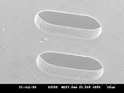
The conventional electroformed stencil manufacturing process involves taking a conductive mandrel such as stainless steel and applying a dry film layer of photoresist. This photoresist layer is then photo patterned and developed. The photoresist addition, high resolution photoresist and photomasks are employed in the process giving a high definition photolithography process. Figures 1a and 1b show characteristic SEM micrographs of the smooth side of the 35µmx80µm electroformed apertures at 60µm pitch. Figures 1a and 1b delineate the smooth side of the stencil which will be in contact with the wafer during printing (“wafer side”). Roughness measurements taken by a Cyberoptics Vantage laser profilometer show a smooth side roughness of 0.11µm and 1.1µm for the 60µm pitch and 100µm pitch stencils, respectively. Correspondingly, the rough side of the stencils which is going to be the paste (“print side”) is dependent on the nickel grain structure and has been found to have a roughness of 0.73µm and 0.83µm for the 60µm and 100µm pitch stencils, respectively. Laser-cut steel stencil of 30µm thickness at 100µm pitch has only a slight better smoothness of 0.51µm of the “print side” than the electroformed stencil. Cross-section views of the electroformed stencils at 60 µm and 100µm pitch are shown in Figures 3 and 4, respectively.
Some paste crawling under the stencil. Nevertheless, it does not seem to be so critical in the 100µm pitch stencil and more importantly does not exist in the 60µm pitch stencil where paste smearing would be even more crucial than in 100µm pitch wafer printing.
Further improvements in Ultra-Fine-pitch electroformed stencil fabrication
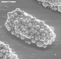
The manufacturing of the thin stencils in this study has pointed out the promising future for electroformed stencils for UFP printing. Further optimisation in the photolithography parameters will yield improvements in the profile of the aperture sidewalls. Excellent results have already been properties of both pastes are similar since it was decided by the manufacturer to use the same chemistry for the newly type 8 as for the standard type 6 paste. The viscosity of both pastes at a shear rate of 10/sec is 240 ± 50 Pa sec. Figure 5 shows print deposits at 60µm pitch on monitor wafer after short heating for flux evaporation. The powder size of type 8 paste has been confirmed


