Abstract
This article provides a multiphase monolithic buck solution to solve high current, fast transient requirements of building a power supply for processing unit. The novel low output noise technology known as Silent Switcher® 3 architecture is introduced and its ultrafast transient feature is utilized in multiphase opera- tions. The unmatched high control bandwidth helps this solution to use fewer output capacitors than others and allows the power supply to achieve very fast recovery time during the transient. Detailed design tips and considerations are covered in this article to help engineers with future designs.
Introduction
Power consumptions for CPUs, FPGAs, and ASICs in today’s computing environ- ment are growing increasingly. And in some more specific applications, such as 5G transceivers, beamformers, and other high speed RF applications, the power requirements are even more strict in terms of the bandwidth and RF noise level. Due to the high output current, the traditional two stage (buck + LDO) solution that is widely used by the RF applications is bulky, not efficient, and requires more heatsinking. The growing requirement for the output current capability makes it uneconomic to use a single buck regulator to power the high demanding load too. Multiphase buck regulators are widely used in this area thanks to the high performance in current delivering capability benefiting from the scalability and ripple interleaving advantage. However, to achieve fast transient and ultralow RF noise requirements, a multiphase buck regulator will require many output capaci- tors and multiple stages of LC filters to fulfill the purpose of powering high speed RF ASICs. The additional components usually use up a significant portion of board space and can potentially increase the solution cost. This article will demonstrate the benefits of using a high performance Silent Switcher 3 architecture, which features in ultralow noise and ultrafast transient in the multiphase buck applica- tions. Different ASIC load requirements will be addressed with different design considerations in the article.
The Silent Switcher 3 architecture features an ultralow noise design (typically 4 μV rms from 10 Hz to 100 kHz), ultralow EMI emissions, and ultrafast transient response with a high gain error amplifier. Among this new product family, the LT8627SP features the highest 16 A current rating, which makes it a perfect can- didate for a multiphase buck configuration in any high current, noise sensitive applications. Due to the low supply voltage nature of all ASIC loads (<1 V) and the widely used 12 V power distribution system, a multiphase buck is very sensitive to the minimum on-time. The innovative architecture of Silent Switcher 3 technology provides the smallest on-time (15 ns), which allows the LT8627SP to easily operate at a switching frequency >1 MHz that benefits to the ripple, size, noise, and bandwidth.
Transient Recovery Time Minimization for a 50 A Current RF Digital Load
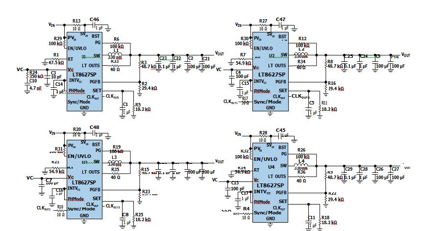
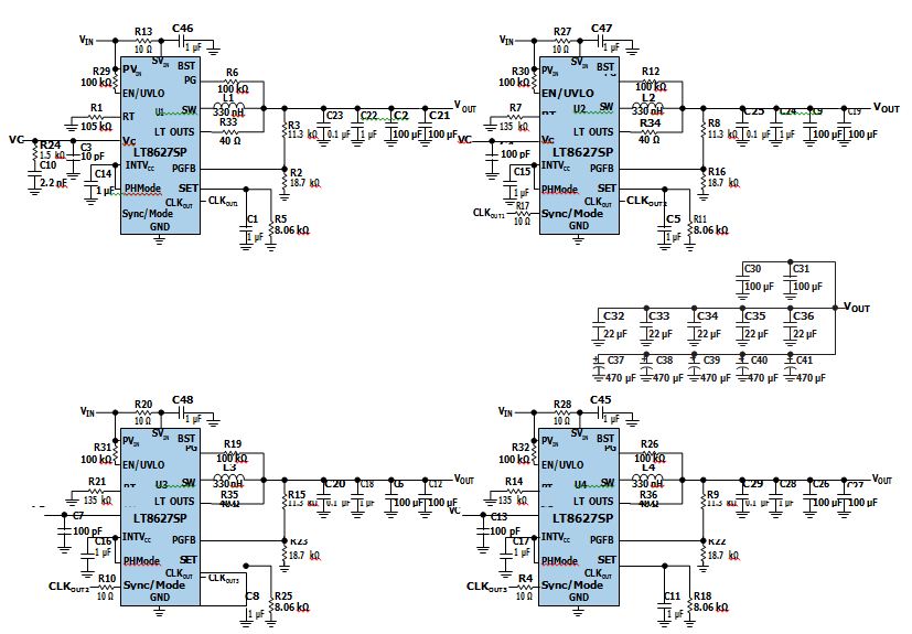
An important characteristic of a power supply’s performance is its recovery time. This is the time it takes for its output voltage to return to its regulated value when a load transient happens. Every power supply has a limit to how fast it can recover, and it is related to its control loop bandwidth. A higher control loop band- width means the inductor current can ramp up/down faster during the transient to compensate for the charge change on the output capacitors to recover in a shorter time. One example of using a four-phase LT8627SP is to power a 1.8 VOUT RF digital load with a maximum load current of 50 A as shown in Figure 1. The power supply was designed to output 1.8 V with a switching frequency of 2 MHz. To shrink the charge compensation time during a transient, low ESR ceramic capacitors are used and high ESR polymer capacitors and electrolytic capacitors are avoided in the design. Interleaving PWM technology (90° per phase) is applied to increase the equivalent ripple frequency so that the control bandwidth can be pushed higher.
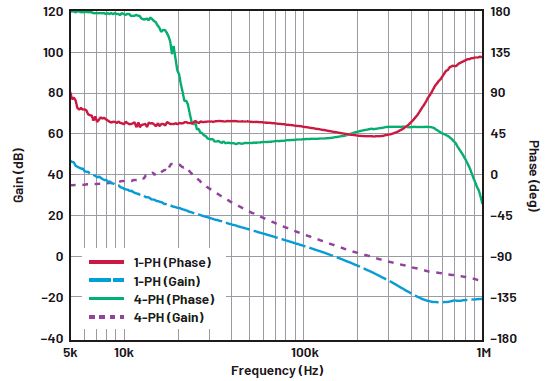
The compensation network is adjusted aiming to achieve at least a 45° phase margin and a gain margin greater than 8 dB while pushing the bandwidth as high as possible. As a result, its control loop was tuned to its highest bandwidth of 280 kHz with 45° of phase margin and 9 dB of gain margin, as shown in the bode plot in Figure 2. As a comparison, a single-phase LT8627SP with equivalent output capacitance per phase (2 × 100 µF + 1 × 1 µF + 1 × 0.1 µF) was tested at 1.8 V, 12 A output. The bode plot is also shown in Figure 2 with the same stability criterion.
Single Phase vs. 4-Phase LT8627SP Bode Plot
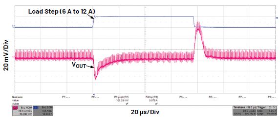
To comparatively test the recovery time, a 50% load transient was performed for both four-phase and one-phase LT8627SP with a slew rate of 6 A/µs per phase. Results shown in Figure 3, a recovery time of around 2.5 μs at the rising edge of the transient. This is almost a 10-fold reduction in recovery time shown in Figure 4 for one-phase LT8627SP.

Transient VPP Minimization for High Current Wireless Applications
The multiphase operation of the Silent Switcher 3 architecture has been used on many customer power supply designs. Figure 5 shows another example of how the LT8627SP is helping a wireless customer power a fast, high current transient SoC with a 0.8 VOUT and 22 A to 60 A load transient in 1 µs. To prevent the SoC performance from downgrading due to the transient, a VPP of less than 5% (40 mV) is desired.
From the previous section, we already know that for four-phase interleaving the LT8627SP, we can expect a fairly high control bandwidth, which is around 300 kHz. And in the time domain, we can roughly model the relationship between the volt- age deviation during the load transient and control bandwidth by:

Thus, we can get the minimum output capacitance to be 1583 µF giving a 10 mV ripple voltage. The design should select capacitance higher than this value and different from the previous section, more polymer capacitors are used to provide enough damping during the transient. The final output capacitance is decided by trial and error as the output capacitance also affects the loop bandwidth and stability.
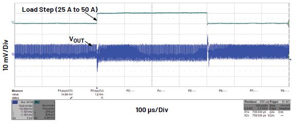
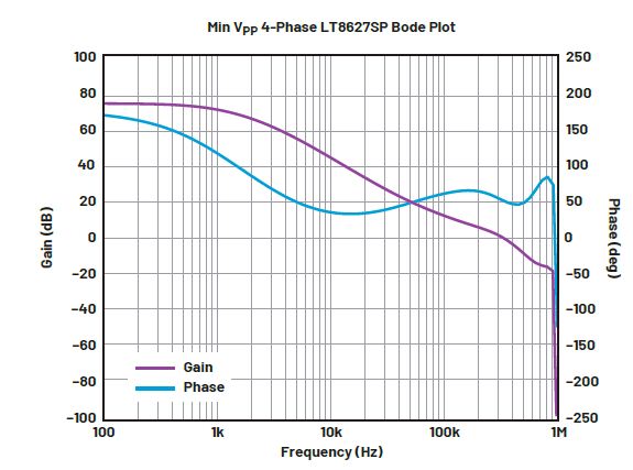
The four-phase LT8627SPs are interleaved at a 1 MHz switching frequency to a combined 4 MHz ripple frequency. And after determining the minimum amount of output capacitance, a 35 mV (4.4%) VPP was achieved in a 22 A to 50 A to 22 A load transient with a 28 A/µs slew rate. The transient waveform is shown in Figure 6. To verify the stability of the control loop, a bode plot measurement was made using a 50 A load. The results are shown in Figure 7. At 50 A, the control loop had a bandwidth of 322 kHz with a 50° phase margin.
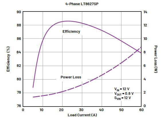
For additional performance tests, the efficiency and full load thermal performance was measured. The efficiency was tested up to a 60 A load at 12 VIN, at 0.8 VOUT as shown in Figure 8. Including auxiliary losses, the converter’s peak efficiency at a 25 A load was 89%, and the converter’s efficiency at 60 A load was 84%.
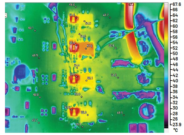
The thermal performance of this four-phase design is shown as a thermal image in Figure 9. At a 60 A load, the hottest IC is 66°C and the coolest IC is 61.6°C. This gives a max temperature deviation of ~5°C between the four ICs, which repre- sents excellent current sharing between phases.
Design Considerations and Guidance for Multiphase LT8627SP
As a peak current mode control IC, the LT8627SP can be easily configured into a multiphase operation. Several design considerations that need special care are:
- For proper current sharing, the VC pins of each IC should be tied together, as shown in the schematic in Figure 1.
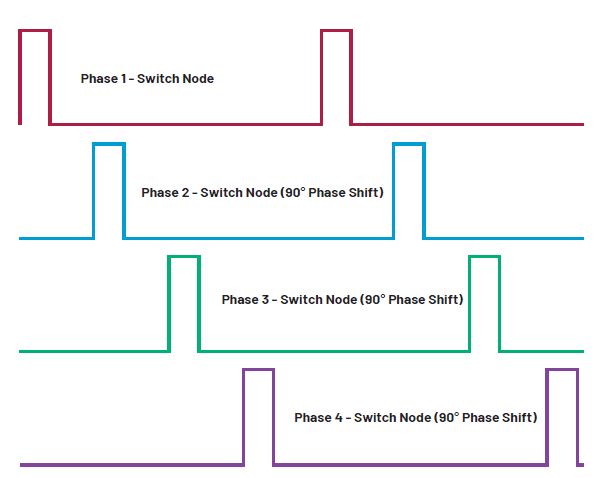
- To evenly interleave for a four-phase LT8627SPs, the CLKOUT of each IC is configured to be 90° phase shifted and fed into the SYNC pin of the next IC. In this configuration, the switch node waveform for each IC is shown in Figure 10. Interleaving is one of the biggest benefits brought by the multiphase buck. As the evenly interleaved phases multiply the output voltage ripple frequency, the output capacitance can be significantly reduced. The higher interleaved ripple frequency can also help the control loop be immune to ripple noise at a higher bandwidth. The LT8627SP can operate up to a 4 MHz switching frequency with three different phase shift clock configurations: 180°, 120°, and 90°. This means it can achieve up to 12 of interleaving without extra devices.
- For proper voltage sensing, the OUTS pins of each IC should be tied together. It is worth noting that since all the error amplifiers (EA) are involved in the control loop, the bode plot injection needs to involve all EAs. As a result, both the sensing point (output voltage) and the OUTS pins side need to be tied together to make sure evenly perturbation is observed for each EA.
- RT pin needs a resistor to set the frequency. The master IC should have a resistor value that sets the desired switching frequency, and the slave ICs should have a resistor value that sets their frequencies 20% lower than the main IC.
Conclusion
Building power supplies for 5G telecom applications can be challenging. The appli- cations require fast, high current transient responses to either achieve minimum peak-to-peak output voltage or minimum recovery time during a load transient. One easy solution to the challenges is to parallel multiple Silent Switcher 3 architec- ture, such as the LT8627SP, power converters into a single interleaving system. By doing so, the bandwidth and load capability of the power supply can be increased, thus its ability to perform fast, high current transients can be achieved.
About the Authors
Erik Lamp is a product applications engineer in the Industrial and Multimarket Group at Analog Devices who specializes in power products. He received his Bachelor of Science in electrical engineering from San Jose State University in 2020 and started his career at ADI that same year. Xinyu Liang is the applications engineering manager in the Industrial and Multimarket Group at Analog Devices focusing on power products. He received his Ph.D. degree in electrical engineering in 2018 from North Carolina State University and he started his career at ADI in 2019 after graduation.


