Abstract
The active clamp forward converter is a recognized high efficiency power topology utilizing P-channel MOS for clamping. This design allows for feedback of stored inductance energy to the grid, enhancing overall converter efficiency. To further improve efficiency, a secondary circuit featuring a MOSFET-based self-rectified circuit is incorporated. This article delves into the design challenges of the secondary rectified circuit, highlighting the role of duty cycle optimization. It’s important to note that this is just one facet of the broader power technology employed in the active clamp forward converter.
Introduction
In an active clamp forward converter (ACFC), the duty cycle is a critical parameter for output voltage and efficiency. Typically, the maximum duty cycle of a forward converter is limited to 50%. With the active clamp technique, it allows the duty cycle to exceed the traditional 50%. There are many articles that have docu- mented the relationship between the maximum duty cycle and ACFC topology, but not many have discussed how to design the minimum duty cycle.
One isolated ACFC power supply is introduced in this article as an example to explain how the minimum duty cycle impacts the design. It is intended for con- verting 24 VAC or 48 VDC to 60 VDC with a delivery capacity of 1.5 A. Its isolation feature makes it suitable for powering industrial applications in the field. The ACFC topology contributes to achieving a peak efficiency of up to 91%. The design requests are shown in Table 1.
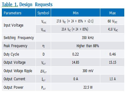
Analog Devices’ MAX17598 serves as an active clamp current mode PWM control- ler, encompassing all control circuits necessary for designing an isolated forward converter power supply. This article delves into the considerations and evaluation results for the secondary self-rectified circuit design.
Design Consideration on the Secondary Self-Rectified Circuit
The ACFC could supply a higher efficiency by using a self-rectified circuit. Figure 1 shows a typical schematic of a MOSFET-based self-rectified circuit. Compared to a traditional diode rectified circuit, the MOSFET has lower ON resistance. This could lead to a higher efficiency, especially in the case of low voltage but high current output.
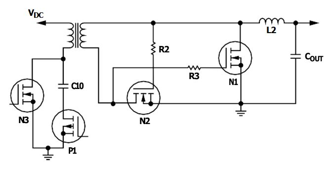
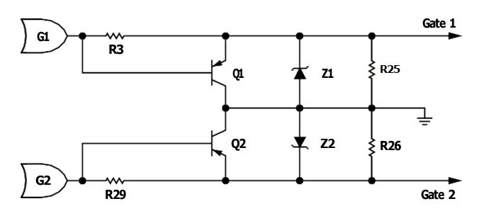
However, it is unsuitable when the output voltage is close to or over the MOSFET gate voltage operation range. An additional circuit can be designed to generate the gate driving voltage of these MOSFETs. Figure 2 shows the details of the circuit. G1 and G2 are connected to the auxiliary winding of the transformer.
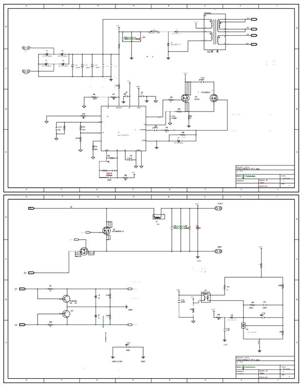
Gate 1 is linked to the gate of N2 (shown in Figure 1), and Gate 2 is linked to the gate of N1. Gate 1 and Gate 2 are synchronized with the switching cycle. When Gate 1 outputs high, Gate 2 outputs low, and vice versa. The full circuit can be found in Figure 3.
This loop must ensure the output is in the operation range for MOSFET VGS. Equation 1 shows the relationship between the gate driving voltage and the turns ratio.

KGATE is the transformer ratio. NG is the turns of the transformer winding. NP is the turns of the transformer primary winding. VGATE_MAX is the maximum voltage of the MOSFET gate driving voltage. VDC_MAX is the maximum voltage of the DC input voltage.
When the main switch at the primary loop is ON, the voltage applied to the trans- former is positive, which is the VDC. The output of Gate 1 is high and Gate 2 is GND accordingly. It is related to the turns ratio and the DC input voltage.

When the main MOSFET is OFF, the clamp circuit will limit the drain voltage to be VCLAMP. Because VCLAMP is higher than VDC, the output of Gate 1 is GND and Gate 2 is high.
The clamp voltage can be calculated as:

The voltage for Gate 2 is related to the turns ratio and the gap between VCLAMP and VDCINPUT.

Since the duty cycle changes with the input voltage, it is essential to ensure the gates’ driving voltage can drive the MOSFET with the full VIN range. Especially, when the maximum DC input and minimum ON rate is applied, the gate driving voltage will reach the minimum value.
In the design example, the lowest Gate 2 voltage can be calculated as shown in Equation 5. When the input DC voltage reaches the maximum value, the voltage on Gate 2 is only 4.23 V.

If this voltage is lower than the VGS ON threshold, the MOSFET of the secondary rectified circuit will not work accurately. This could lead to an issue in which the power supply cannot start up without any load when the input voltage is close to the maximum value. In the example circuit, the VGS threshold voltage is 3 V, which is less than the minimum VGATE2 calculated.
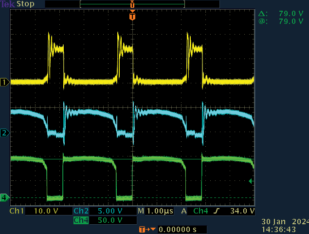
Figure 4 shows the measurement result on the example circuit. CH1 shows the voltage of Gate 1. CH2 shows the voltage of Gate 2. CH4 shows the source-drain voltage of the N-MOS at the primary side.
Performance of Example Circuit
To verify the accuracy of our calculations for the gate drive circuit, we conducted performance tests on the example circuit. Figure 5 shows the input and output voltage with different load currents of 0 A, 0.5 A, 1 A, and 1.5 A.
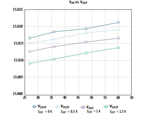
Figure 6 shows how the output voltage level changes with a different output current. Different lines show the different input voltage.
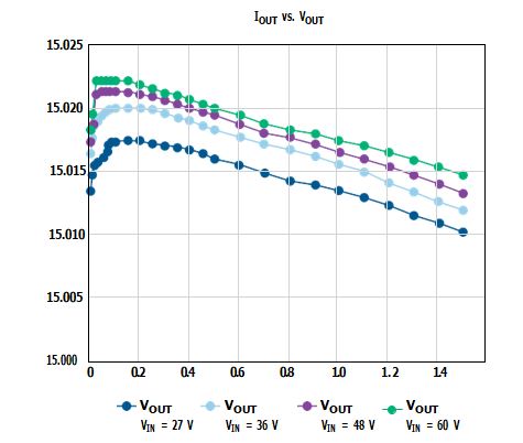
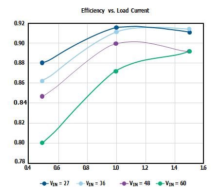
Figure 7 shows the peak efficiency by different input voltages and loads. The peak efficiency reached 91% when the input is 36 V with 1.5 A output.
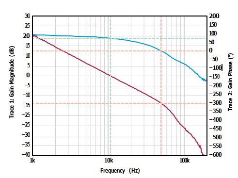
The Bode plot shows the loop stability at the working condition of peak efficiency,
which is VDCINPUT = 36 V, IOUTPUT = 1.5 A.
Figure 8 shows the loop response.
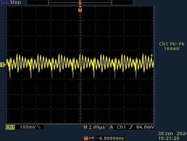
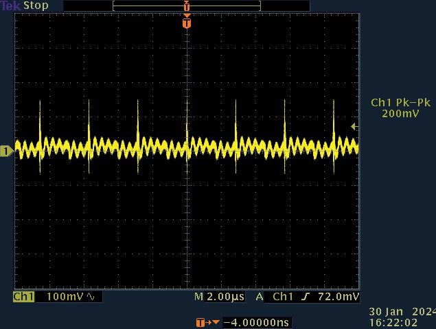
Figures 9 and 10 show the output peak-to-peak voltage. Figure 9 is without load current and Figure 10 is the result with full load.
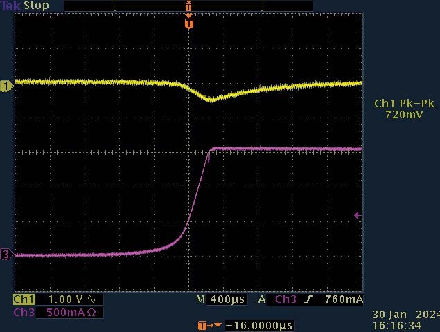
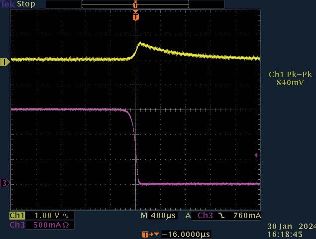
Figures 11 and 12 show the load transient response. Figure 11 shows the load changed from zero to full. Figure 12 shows the load changed from full to zero. CH1 measured the output voltage (AC-coupled). CH2 measured the output load current.
Conclusion
In conclusion, the study on ACFCs has revealed significant insights into their per- formance and efficiency. By examining the secondary rectified circuit design and the impact of the duty cycle, it has been demonstrated the limits of minimum duty cycle when an additional auxiliary gate drive circuit is requested.
Furthermore, the ACFC with its unique ability to recycle energy stands out as a promising solution for high efficiency power supply systems. Through this article, it is evident that there is an optimal range for duty cycle. Not only the maximum duty cycle but also the minimum is important for MOSFET-based rectified circuits.
Incorporating the findings from this study into the design and implementation of ACFCs could lead to avoiding problems during the design phase.
Reference
1“Designing Active-Clamp Forward Converters Using Peak-Current-Mode Controllers.” Analog Devices, Inc., August 2014.
About the Author
GuangQi Hou received his B.E. degree in electronics and electrical Engineering from Keio University, Japan in 2008. He joined Analog Devices in February 2021. He is working in the China Technical Support Team and focusing on products related to fuel gauge, power management, industrial interface, motor, and motion control.


