Features
- Microcontrollers for industrial, instrumentation, medical, communications, and automotive applications
- Leading edge mixed-signal integration with 12-, 16-, or 24-bit ADCs, multiple
- 12-bit DACs, reference and temperature sensor.
- ARM7TDMI Flash/EE and 24-bit analog-to-digital converters in 5 mm × 5 mm LFCSP
- 3-phase PWM, quadrature encoder, PLA, and up to 128 kB Flash/EE, plus 8 kB SRAM
- Fully integrated solution for automotive battery monitoring (ADuC703x series)
- 8052 MicroConverter series with Flash/EE and 12-bit to 24-bit analog I/O
- Complete suite of development tools
Precision Analog Microcontrollers—ARM7™ and 8051 Series
Analog Devices precision analog microcontrollers combine precision analog functions, such as high resolution ADCs and DACs, a voltage reference, and temperature sensor with an industry-standard microcontroller and flash memory. For example, the ADuC702x ARM7TDMI® family integrates 12-bit analog I/O with flash, SRAM, and a host of digital peripherals. These devices use a single 32-bit bus for instructions and data, integrate a
JTAG test port for debug access, and operate up to 44 MHz. In addition to the 32-bit ARM®
instruction set, the core supports an instruction set that is compressed into 16 bits (Thumb® mode). The on-chip precision analog I/O includes a multichannel 1 MSPS, 12-bit ADC, up to four 12-bit voltage-output DACs, a low drift band gap voltage reference, a temperature sensor, 3-phase PWM, a user-configurable PLA, and an uncommitted voltage comparator. All of this, and more, come in a variety of package footprints with the smallest being a tiny 5 mm × 5 mm, 32-lead chip scale package.
Getting more application specific, the ADuC7128/ADuC7129 extend the ADuC702x series to include a quadrature encoder and PWM for dc motor control applications. They also feature a 32-bit, 22 MHz DDS input followed by a high speed 10-bit DAC and a 100 Ω line driver, useful for transducer excitation.
The ADuC703x series, specifically for automotive battery monitoring, integrates up to three 16-bit ADCs to measure battery voltage, current, and temperature, the required high voltage I/O for direct battery interface, and an LIN transceiver to handle communications to the engine control unit.
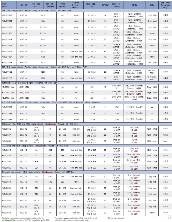
The new ADuC706x series with the ARM7 core, dual and single 24-bit Σ-∆ ADCs, PGA, 14-bit DAC, and precision current sources are particularly suited to direct connection and signal processing in precision sensor and loop-powered applications.
ARM7 Core Products with Precision 12-Bit Analog I/O (ADuC7019 to ADuC7028, ADuC7128, and ADuC7129)
Architectural Overview
The ARM7TDMI core is a 32-bit RISC machine. It uses a single 32-bit bus for instructions and data. The TDMI option provides four additional features: a secondary 16-bit Thumb (T) instruction set, debug (D) support, support for long multiples (M), and includes the embedded ICE (I) module containing the breakpoint and watchpoint registers, which allow code to be halted for debugging purposes.
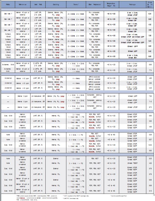
Each ADuC7xxx device operates from an accurate (±3%) on-chip oscillator and PLL generating an internal 41.7 MHz clock that is routed through a programmable clock divider from which the MCU operating frequency is generated. Alternatively, the parts can run from a master clock up to 44 MHz. Power consumption is 1 mA/MHz.
Either 126 kB, 62 kB, or 32 kB of nonvolatile Flash/EE and 8 kB of SRAM are provided on chip with both blocks mapped into a single linear array. ARM code can run directly from SRAM at 41.7 MHz/44 MHz (internal/external clock), given that the SRAM is configured as a 32-bit wide memory array. The 80-lead devices support external memory.
On-chip firmware supports in-circuit serial download via the UART or I2C® and JTAG serial interface ports while nonintrusive emulation is also supported via the JTAG interface.
Key Features
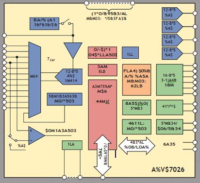
- ARM7TDMI MCU core
- 16-/32-bit RISC architecture, 44 MHz operation
- Embedded JTAG for debug
Memory Organization
- 8 kB SRAM in 2k × 32 bits
- Up to 126 kB Flash/EE in 31k × 16 bits
- Retention: 20 years
- Endurance: >10k cycles
- In-system programming (ISP) via UART, I2C, or JTAG ports
Analog I/O
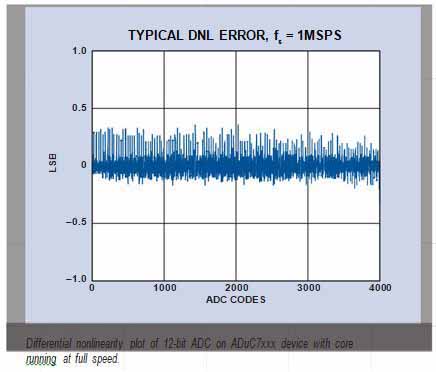
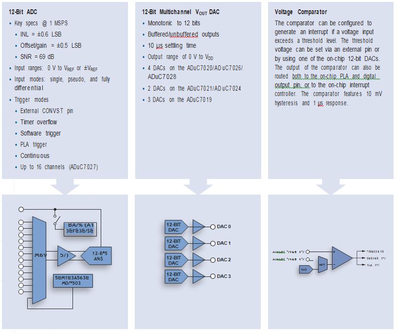
- Multichannel, 12-bit, 1 MHz ADC
- Multiple 12-bit VOUT DACs
- 40 ppm/°C VREF, 3°C temp sensor
- Uncommitted comparator
Additional Features
- 2 × GP timers
- Programmable logic array (PLA)
- UART, SPI, dual I2C, serial I/O
- Up to 40 GPIO pins
- Power supply monitor and power-on reset
- 3-phase PWM
- Specified for 3 V operation (5 V compatible I/O)
- Temperature range: –40°C to +125°C
- 6 mm × 6 mm and 9 mm × 9 mm LFCSP, 64-lead and 80-lead LQFP package options
- 1 mA/MHz current consumption
- Low cost QuickStart™ Development System support
ADuC7xxx Series On-Chip Peripherals
High performance analog I/O and several other peripherals are included on chip. Some of them are examined here. See the selection guide for a complete listing.
Programmable Logic Array (PLA)
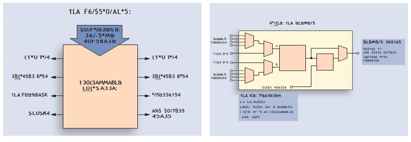
The integrated PLA consists of two interconnected blocks of eight PLA elements for added flexibility. Each element can be configured to generate any logic output function based on two inputs, eliminating the need for external logic gates. The PLA is programmed with run-time code via the standard memory-mapped register (MMR) interface.
ARM7 Series with Quadrature Encoder and H-Bridge PWM for Motor Control
ADuC7128/ADuC7129
The ADuC7128/ADuC7129 combine an ARM7 microcontroller, 12-bit, 1 MSPS ADC, and a 10-bit DAC, along with a 16-bit PWM with H-bridge mode and quadrature encoder. There is a 32-bit, 22 MHz DDS input to the DAC, which also incorporates a 100 Ω line driver. This level of integration benefits designers of brushless dc (BLDC) and instrumentation systems, reducing external component count, while working in a familiar ARM7 environment.
Key Features
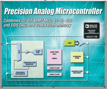
- ARM7 with 126 kB flash
- 10-bit DAC with 32-bit, 22 MHz DDS
- 16-bit PWM generator
- 10-channel, 12-bit, 1 MSPS ADC
- Quadrature encoder
- Temperature range: –40°C to +125°C
Additional Features
- Dual UART
- Differential line driver output
- 64-lead LFCSP package and 80-lead LQFP package (external memory)

DDS DAC Operation
- 32-bit DDS register
- 4096 point table
- 0.005 Hz resolution
- Minimum frequency: 0.005 Hz
- Maximum frequency limited by LPF
- THD: 51 dB typ
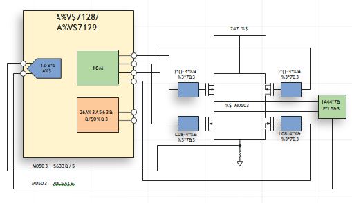
Application Focus: ADuC7128/ADuC7129 in H-Bridge Motor Control
The ADuC7128 integrates a 6-channel PWM interface. The PWM outputs can be configured to drive an H-bridge or can be used as standard PWM outputs. On power-up, the PWM outputs default to H-bridge mode. This ensures that the motor is turned off by default. In standard PWM mode, the outputs are arranged as three pairs of PWM pins. Users have control over the period of each pair of outputs and of the duty cycle of each individual output.
Integrated Battery Sensor for Automotive Battery Monitoring Includes High Voltage Physical Interface for LIN
ADuC703x Family
The ADuC703x family of automotive battery monitor solutions addresses a growing need to monitor and distribute power, and provide priority to critical functions such as engine startup. The ADuC703x family measures elementary physical variables such as battery voltage, current, and temperature to determine the battery’s state-of-charge (SOC) and state-of-health (SOH). The vehicle’s energy management system then uses this data to reserve sufficient battery energy for a guaranteed engine start and to tailor the charging cycles resulting in reduced fuel consumption.
The ADuC703x family integrates an on-chip PGA (programmable gain amplifier) for a wide range of battery current measurements and, similarly, attenuation for battery voltage measurement. Also on board are up to three 16-bit analog-to-digital converters (ADCs), an ARM7 microcontroller, a local interconnect network (LIN) transceiver, and embedded memory in a single package. The devices offer a cost-efficient and space-saving alternative to discrete solutions, which consists of a standalone processor, LIN transceiver, low dropout regulator (LDO), and analog front end (AFE). As a result, the component can be located between the battery terminal and the connector on the main power cable, giving a great saving in space and cost, while simplifying overall battery monitoring system design.
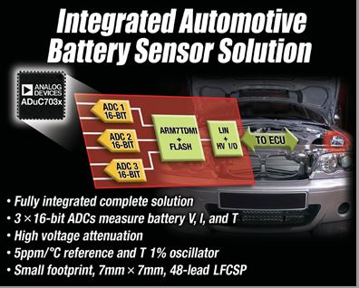
Key Features
- ARM7TDMI MCU core
- Operates from 12 V battery supply
- Low power consumption
- 175 μA in low power mode
- Up to 10 mA at 10 MHz in regular mode
Memory Organization
- 6 kB SRAM
- 96 kB Flash/EE
- Retention: 20 years @ 85°C
Analog I/O
- 3 × 16-bit Σ-∆ ADC
- 5 ppm/°C VREF
- ±2°C temperature sensor
- Digital comparator and integrator
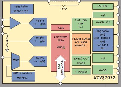
Additional Features
- Programmable gain amplifier (PGA)
- PLL
- Precision oscillator (±1%)
- Timers (watchdog, wake-up, 2 × GP)
- Power supply monitor
- Power-on reset
- LIN (local interconnect network) transceiver
- Temperature range: –40°C to +125°C
- 7 mm × 7 mm, 48-lead LFCSP package
| Part Number | ADCs | Flash (kB) | SRAM (kB) | Timers | Package | Price @ 1k ($U.S.) |
| ADuC7032 | 3 | 96 | 6 | 4 | 48-lead LQFP | 7.55 |
| ADuC7033 | 2 | 96 | 6 | 5 | 48-lead LFCSP, 48-lead LQFP | 7.10 |
| ADuC7034 | 2 | 32 | 4 | 5 | 48-lead LFCSP, 48-lead LQFP | 6.73 |
Application Focus: Electrocardiogram Using ADuC7021
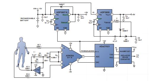
An electrocardiogram (ECG) is the recording of the electrical activity on the body surface generated by the heart. This electrical activity is collected by skin electrodes placed on predetermined parts of the body. A low cost implementation of an ECG monitor is shown in the schematic here, and for the main signal processing, the ADuC7021 MicroConverter device is chosen. This part features the necessary high performance analog peripherals, a fast ARM7 core, integrated 62 kB flash for code, and several other useful peripherals. The ADC converts the analog signal from the differential amplifier to a digital signal. The software, resident in the ADuC7021 flash, then processes the digitized signal to produce the final ECG trace. Because of the flash- based code memory on the ADuC7021, this customization can be done after manufacture or even as the individual patient’s needs change.
For more information, see complete technical article at www.analog.com/library/analogdialogue/archives/37-11/ecg.pdf.
Application Focus: Pulse Oximeter Uses ADuC7024
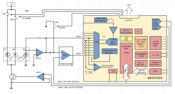
Beyond heart rate, blood pressure, respiratory rate, and temperature—pulse oximetry is considered to be the “fifth vital sign” of health status. A pulse oximeter is a medical device that provides a noninvasive measure of the amount of oxygen in a patient’s arterial blood.
A typical oximetry sensor has a pair of light-emitting diodes (one red with 660 nm wavelength, one infrared with 940 nm wavelength) facing a photodiode through a translucent part of the patient’s body, usually a fingertip or an earlobe. The percentage of blood oxygen is calculated based on the absorption rate from each wavelength of light after it passes through the patient’s body.
The precision analog microcontroller family of products from Analog Devices includes the key analog building blocks required for high end oximetry designs. The ADuC7024, used here, includes a high performance, high speed, multichannel, 12-bit, 1 MSPS ADC and two DACs. The MicroConverter device also includes a 32-bit ARM7TDMI core. Running at 41.8 MHz, it provides a very powerful computational platform for digital signal processing algorithms to detect arterial blood pulsations, while allowing plenty of CPU performance for additional functions, such as control of the graphics LCD display. The ADuC7024 MicroConverter device features 30 general-purpose I/Os (GPIOs), required for interfacing with the LCD. With fewer I/Os, the same level of performance can be achieved by using the ADuC7021, available in a space-saving 6 mm × 6 mm LFCSP package.
For more information, see complete technical article at www.analog.com/library/analogdialogue/archives/41-01/pulse_oximeter.html.
Transceiver Module with SFP and XFP Chipset and Reference Design
Analog Devices’ chipsets and reference designs work together seamlessly and enable designers to develop best-in-class optical transceivers with minimal time and effort. XFP is rapidly becoming the leading standard for optical transceiver modules that connect to 10 Gbps ports, such as those used in Ethernet, Fibre Channel, and SONET/SDH protocol applications.
For more information, visit www.analog.com/xfp_ref_design and www.analog.com/sfp_ref_design. The chipset consists of
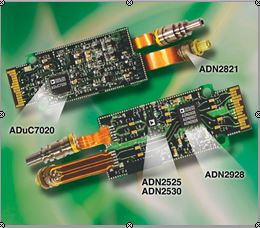
- TIA:
- ADN2821, 11.1 Gbps, 3.3 V, low noise, high gain transimpedance amplifier
- LDD:
- ADN2525, 10 Gbps active back-match, differential laser diode driver
- ADN2530, 10 Gbps active back-termination VCSE driver
- XFP signal conditioner:
- ADN2926/ADN2927, standalone transmit and receive functions in a 4 mm × 4 mm LFCSP
- ADN2928, XFP single chip transceiver IC
- Microcontroller:
- ADuC7020, precision analog microcontroller:
44 MIPS ARM7 flash MCU, 5-channel, 1 MSPS, 12-bit ADC, quad 12-bit DAC, two I2C ports, in 6 mm × 6 mm, 40-lead LFCSP
Energy Measurement IC Integrates ADE Core with 8052 Core
The ADE51xx and ADE55xx energy meter SoC (system on a chip) families provide a cost-effective solution for meter manufacturers by integrating ADI’s proven energy measurement core with the 8052 microprocessor, on-chip flash memory, LCD driver, real-time clock (RTC), and intelligent battery management. The ADE51xx and ADE55xx families have unique battery management features that consume less than 1.5 μA of current in battery mode while keeping critical system components active. Based on ADI’s field-proven ADE energy measurement core that is designed into more than 225 million energy meters worldwide, these highly integrated SoC devices provide a high performance, cost-effective, and low risk solution.
For more information, visit www.analog.com/energymeter.
Features
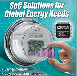
- 4-quadrant high precision energy measurement
- Battery operation down to 2.4 V power supply
- Power fail/battery management with no external component needed
- 104-segment LCD driver
- Low power RTC—1.5 μA typical
- RTC compensation accurate to 2 ppm
- Digital temperature measurement
Benefits
- Single chip solution
- No external battery switching circuitry required
- LCD display maintained in battery mode
- Extended battery life with low voltage operation
- Integrated LCD contrast adjustment

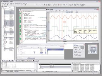
QuickStart Development Tools for ADuC7xxx Series
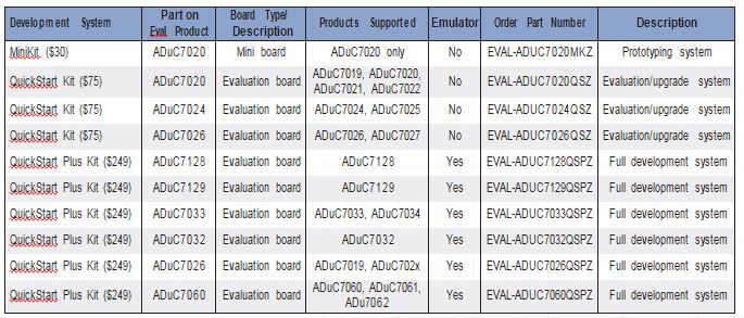
All ADuC7xxx series precision analog microcontroller products are supported by a comprehensive suite of software development tools that are shipped with supporting hardware. The ADuC7xxx series low cost QuickStart Development System includes a suite of software development tools by Keil Software and IAR Systems. The hardware includes a power supply, cables, an evaluation board, and an RDI-compliant JTAG emulator. The QuickStart Development System is priced at $249 (with emulator) and at $75 (without emulator) and is available directly from Analog Devices.
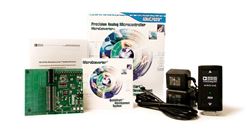
All you need to get started:
- Evaluation board
- ADI mIDAS-Link JTAG emulator
- Power supply
- Serial download cable
- Keil μVision3 IDE (16k limit)
- IAR Systems WorkBench for ARM (32k limit)
- Serial downloader
- PLA tool
MiniKit—ADuC7020
For a rapid start with the ARM7TDMI-based precision analog microcontroller, Analog Devices is offering a very low cost evaluation kit, the ADuC7020 MiniKit. This is a small adapter board with the form factor of a standard 40-lead DIL-socket. It is powered directly from a 9 V battery block and can be connected to a PC with the included serial
download cable. In addition to the evaluation software package, it comes with a comprehensive installation and getting-started presentation on CD, to enable the user to debug code in the on-chip flash memory. This low budget evaluation tool enables the user to experience the quality of the high performance 12-bit analog front end (12-bit/1 MSPS ADC and 12-bit voltage output DAC) in combination with the powerful processing capabilities of the 32-/16-bit ARM7TDMI core and the integrated real- time-programmable logic array (PLA).
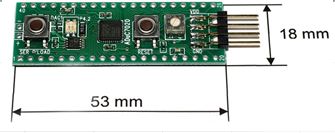
- The MiniKit consists of
- Mini board
- Power supply cable
- Serial download cable
- Keil μVision3 IDE (16k limited)
- Compiler/simulator/debugger
- IAR Workbench IDE (32k limited)
- Compiler/simulator/debugger
- Serial downloader
- PLA tool
- Example code
ADuC8xx Series: 8052-Based MicroConverter Products
The ADuC8xx series was the first to integrate true 12-bit to 24-bit analog precision, in-circuit reprogrammable Flash/EE memory, and an on-chip 8052 core. Applications include industrial control, precision instrumentation, and communications infrastructure. Options with high resolution Σ-∆ ADCs, such as ADuC845, ADuC847, and ADuC848, are particularly suitable for applications that call for precise measurement of low frequency signals with a wide dynamic range. Examples include intelligent sensor calibration and conditioning, smart transmitters, weigh scales, temperature and pressure transducers, 4 mA to 20 mA control loops, patient monitoring equipment, and portable test-and-measurement gear.
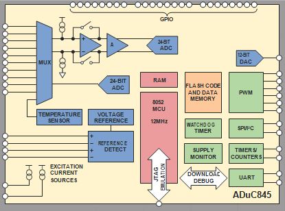
Precision Analog
- 12-bit to 24-bit ADC resolution
- Sample rates to 400 kSPS
- Flexible ADC input multiplexing
- Programmable gain differential inputs
- Self-calibration
- On-chip 2.5 V band gap reference
- Single or dual, 12-bit rail-to-rail DAC
Integrated Programmable Peripherals
- 8052 MCU core (up to 20 MIPS)
- Flash code memory (up to 62k)
- Flash data memory (up to 4k)
- RAM (up to 2k)
- Flexible SPI, I2C, and UART serial ports
- High speed baud rate generator
- Multiple PWM outputs
- Watchdog timer
- Power supply monitor
- Robust internal POR
Essential Embedded Tools
- Serial port downloader/debugger
- Single pin emulator
- Code lockout security feature
Additional Features
- TSSOP, MQFP, and CSP packages
- Extended temperature range to 125°C
- Pin-compatible upgrade paths
- 3 V and 5 V operation
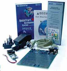
QuickStart Development Tools ADuC8xx Series
The “entry level” QuickStart Development System allows designers to rapidly evaluate MicroConverter performance and functionality, and then begin a prototype development. The system provides all of the tools needed, including software tools, development board, integrated serial download/debug cable, and power supply. It fully supports assembly level code development via a serial port debug path and provides designers with access to a demonstration project of the C-level development environment available in QuickStart Plus.
A small, nonintrusive, single-pin emulator POD and the accompanying Aspire™ Integrated Development Environment (IDE) are supplied directly by Accutron Ltd. and can be ordered via the company’s website.

Precision Analog Microcontroller with Unequalled Data Acquisition and Processing Performance for Industrial and Instrumentation Applications
ADuC706x Family
The ADuC706x family of ARM7 microcontrollers with best-in-class data conversion performance is ideal for industrial systems engineers designing smart sensing, factory automation, and instrumentation equipment.
ADuC7060 incorporates two 24-bit Σ-∆ ADCs and a host of analog peripherals with ARM7 core to create a solution for precision sensing applications. The integration of a 32-bit RISC MCU, flash memory, and high resolution data converters in a small footprint, combined with low power operation eliminates the complexity, cost, and performance degradation issues associated with discrete mixed-signal solutions.
Designed to support 4 mA to 20 mA loop-powered applications and precision instrumentation, the 24-bit Σ-∆ ADC provides the resolution required by high performance industrial and instrumentation equipment, while keeping the noise low at just 60 nV. This performance combined with an ARM7 provides a single chip solution that can handle all data acquisition, processing, and communications functions at the sensor node.
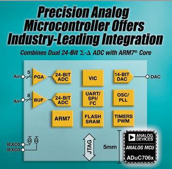
In addition to the 5-channel, 24-bit Σ-∆ ADC with PGA and the ARM7 core with eight interrupt priority levels, the ADuC706x products integrate 32 kB flash memory and 4 kB SRAM, a 14-bit DAC, multiplexers, buffers, an auxiliary 8-channel, 24-bit ADC for cold junction compensation in thermocouple applications, and SPI, UART, and I2C ports. Operating current is just 2.6 mA with all peripherals activated.
Key Features
- ARM7TDMI MCU core
- Low power consumption
- 2.6 mA with all peripherals activated
Memory
- 4 kB SRAM
- 32 kB Flash/EE
Analog I/O
- 2 × 24-bit Σ-∆ ADC
- 14-bit DAC
- 10 ppm/°C VREF
- 3°C temperature sensor
Additional Features
- Programmable gain amplifier (PGA)
- Precision oscillator (±1%)
- Timers (WDT, wake-up, PWM)
- VIC (vectored interrupt controller)
- 2× excitation current sources
- Temperature range: –40°C to +125°C
- 5 mm × 5 mm, 32-lead LFCSP package
| Product Number | 24-Bit ADCs | AINs/GPIOs | Flash (kB) | SRAM (kB) | Package | Price @ 1k ($U.S.) |
| ADuC7060 | 2 | 13, 16 | 32 | 4 | 48-lead LFCSP, 48-lead LQFP | 4.90 |
| ADuC7061 | 2 | 13, 8 | 32 | 4 | 5 mm × 5 mm, 32-lead LFCSP | 3.95 |
| ADuC7062 | 1 | 5, 8 | 32 | 4 | 5 mm × 5 mm, 32-lead LFCSP | 3.40 |


