All the devices we use, right from smartphones to smart automobiles, depend on microscopic chips that enable various functions. But do you ever wonder how these chips transform from a blueprint into the powerful, efficient units within your devices? Semiconductor assembly and packaging equipment holds the key, taking care of everything from installing microscopic components to encapsulating and connecting them for optimum performance.
What is Semiconductor Assembly and Packaging Equipment?

Semiconductor assembly and packaging equipment involves the instruments and technology to assemble, test, and package semiconductor chips once they have been produced. The procedure involves mounting microchips onto substrates, wiring them or other devices together, and sealing them into protective containers to keep them operating efficiently and ready for application in electronic appliances. The packaging also helps to shield sensitive circuits against environmental degradation while promoting heat transfer and electrical connectivity. This critical step means that semiconductors are able to function reliably in everything from smartphones to high-end computing systems.
Types of Semiconductor Packaging
Semiconductor packaging is an essential process in the manufacture of chips as it assures their reliability, functionality, and integration in any electronic device. Some of the most widely used semiconductor packaging types include:
Traditional Packaging
Conventional semiconductor packaging, such as dual-in-line packages (DIP) and lead frame packages, entails mounting the semiconductor die (chip) on a metal frame and wire bonding it. This form of packaging has existed for decades and is still very common for low-to-medium complexity devices such as microcontrollers and basic integrated circuits.
Flip-Chip Packaging
In flip-chip packaging, the semiconductor chip is oriented face down and the active side towards the substrate. The chip is bonded directly to the substrate with solder bumps or microbumps. Flip-chip packaging is advantageous in that it offers high-density interconnections and high performance and is ideal for application in high-speed processors, graphics chips, and memory. Flip-chip packaging guarantees improved thermal management and electrical performance.
System-in-Package (SiP)
SiP integrates different chips and elements, including passive devices, into one package. Through such packaging, it is achievable to fabricate intricate systems without the need for many individual packages, thereby occupying less space and rendering the system smaller as a whole. SiP has broad applications in mobile phones, wearables, and other miniaturized electronic systems in which space and power consumption are factors of importance.
Fan-Out Wafer-Level Packaging (FO-WLP)
Fan-Out Wafer-Level Packaging (FO-WLP) is a next-generation packaging technology with the semiconductor die mounted onto a wafer containing a larger set of connections, spreading out over the chip’s physical area. This technology can provide additional I/O connections and improved performance while still keeping the profile thin. FO-WLP is increasing its adoption in the consumer electronics and smartphone industries for the compact, high-performance packages with improved reliability.
3D Packaging
3D semiconductor packaging stacks multiple chips vertically into one package, which minimizes space and maximizes performance. This method is especially beneficial for users with high bandwidth requirements and low latency, including in-memory computing and high-performance computing (HPC). Stacking chips, 3D packaging maximizes space and raises overall processing power, allowing for more complex and efficient systems.
Semiconductor Assembly and Packaging Equipment Industry Insights
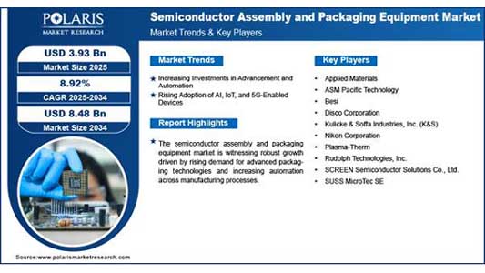
- The global semiconductor assembly and packaging equipment market was valued at USD 3.62 billion in 2024.
- The market is expected to register a significant CAGR of 8.92% from 2025 to 2034.
- By 2034, the market is projected to reach USD 8.48 billion.
- The demand is driven by the increasing need for advanced packaging solutions, growing investments in technology and automation, and the rapid adoption of AI, IoT, and 5G devices that require high-performance chips.
View More Information @ https://www.polarismarketresearch.com/industry-analysis/semiconductor-assembly-and-packaging-equipment-market/request-for-sample
What’s Driving the Future of Semiconductor Packaging?
The future of semiconductor assembly and packaging is shaped by developing smaller, faster, and more efficient chips. 3D packaging is becoming popular, allowing chip stacking that improves performance and efficiency in space, which is essential for AI and high-performance computing. New materials and fan-out wafer-level packaging (FO-WLP) are leading to density and thermal management, vital for next-generation products like 5G smartphones. Additionally, the implementation of AI and automation at the packaging level is improving speed, accuracy, and cost savings.
Final Thoughts

The semiconductor assembly and packaging equipment market is at the heart of the technology that drives our modern world. From smartphones to AI-powered devices, the chips in them are optimized and made efficient due to advanced packaging methods. With growing demand for high-performance chips, the market is changing speedily, fueled by innovation in the form of 3D packaging, automation, and advanced materials.
Read More @ www.polarismarketresearch.com