Stencil printing is one the main process in SMT Production line. Stencil Printing is used in the electronic packaging industry primarily to generate the mechanical and electrically conductive interconnects between two devices. The devices themselves can be pre-packaged chips, individual die, wafers, discrete devices and substrates such as PCBs, flex substrates or ceramic multi-layer circuits.
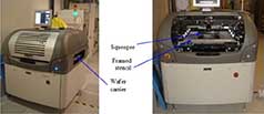
In a modern stencil printing machine for electronic packaging the stencil is normally located in the front of the machine, with the squeegees positioned above the stencil, as shown in Figure 1.
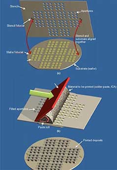
The substrate carrier is then passed through the side of the machine and subsequently aligned to the stencil. During the printing process the substrate is brought into contact or proximity with the stencil. The squeegees are placed onto the stencil with a set pressure and driven across the surface of the stencil at a pre-defined speed. This action causes the paste material to roll across the stencil and the apertures on the stencil are filled with a viscous material, usually solder paste or an isotropic conductive adhesive (ICA). When the stencil is released from the substrate the resulting contents of the filled apertures are ideally transferred to the bond pads, thereby forming deposits that will create the interconnects. With one print stroke, millions of deposits can be placed simultaneously onto the substrate surface. This process, that takes place within seconds, can be repeated thousands of times with the same stencil onto subsequent substrates, thereby creating a low cost, high throughput process. Photographs of a modern stencil printing machine are shown in Figure 2.
Consumer demand for lighter, cheaper, smaller and smarter electronic products is pushing the electronics industry to utilize the smallest packaging footprint possible. In this respect, flip-chip packaging is seen as the ideal platform to satisfy the drive for faster and denser electrical input/outputs, gaining, thereby, an increasing level of acceptance for many industrial sectors covering automotive, consumer and telecommunication applications (Ginsberg, 1989). Stencil printing for flip-chip packaging offers a cost reduction in packaging over competing technologies while, at the same time, preserving the increased package density and reliability improvement that flip-chip bonding provides.
Stencil Technology
There are three main existing conventional stencil manufacturing methods with hybrid variations within each process:
1 Chemical etched stencil.
2 Laser cut stencil and
3 Electroformed stencils.
Laser cutting and chemical etching are both subtractive processes, where the surface texture of the stencil is determined by the material selection. Electroformed stencils are based on an additive process and, therefore, the final surface texture is determined by the electroplating process. The use of nano-coatings on stencils has the potential to impact printing performance and, in recent years, has gained more widespread use.
Hybrid Stencils
There are a number of stencil processes, which take elements of the three different stencil manufacturing processes described above. Step stencils are used when the substrate has a raised area such as a plug or socket on a PCB and therefore the stencil must conform to the surface. In addition, step stencils can be used when there is a high component mix of large and fine pitch devices whereby a stencil can be used to print different pitches or a complicated pattern more easily. Such stencils can be fabricated by a number of different means as shown in Figure 7. Step etching is where the pockets are formed on one side of the stencil and the apertures on the other. The apertures for the regions not containing the pockets can also be patterned and etched from both sides. Step stencils can also be produced by etching the pockets and subsequently laser cutting the apertures. Another technique to generate such step stencils can be through milling either just the pockets or, for course geometries, both the pockets and the apertures. It is, however, more common to mill the conductive substrate with the pockets and then electrochemically form a step stencil onto the substrate. Normally, the stencil apertures are subsequently laser cut.
Nano Coatings for Stencils
In recent years functional nano-coatings have been trialled on the apertures as well as the substrate side of stencils. The idea is to modify the surface characteristics of the stencil so that flux in solder paste is repelled from the aperture sidewalls to minimise the amount of material that is adhered to the apertures after printing. In addition, the coating is also used to stop paste spreading on the underside of the stencil, which reduces the underside stencil cleaning frequency, and also lowers defect rates. To date the limited investigations on nano-coated stencils have shown improved performance, especially on electroformed stencils and higher aspect ratio apertures.
Stencil Printing Factors
Several factors determine the outcome of the print results and these are:
• Stencil: Tensioning, aperture size, roughness and quality, dimensional tolerances, thickness, thickness uniformity, stencil surface texture and stencil material.
• Printing material: Material selection and rheology.
• Environmental conditions: Temperature, noise, humidity and air cleanliness.
• Print parameters: Print speed, print pressure, print gap, separation speed and print direction.
• Squeegees: Squeegee technology, squeegee material and squeegee angle.
• Alignment accuracy between the stencil and the substrate.
• Framing of the stencil.
• Substrate: Flatness, roughness, surface wetting characteristics, bond pad size and shape.
• Substrate support and substrate carrier.
Printing Environment Conditions and Print Parameters
A controlled printing environment is necessary at finer dimensions for a stable and repeatable printing process. All environmental factors such as air cleanliness, background noise, humidity and temperature have an increasing influence on the results of the printing process. In that regard, most stencil printing machines used in flip-chip and wafer level packaging are located in some form of cleanroom environment of class 10,000 at least, with temperature, humidity and air cleanliness control and for some applications, vibration isolation.
In contrast, most SMA lines are today typically found on the factory floor with just temperature control. Printing parameters are specifically tailored to the printing pitch, stencil technology and paste material selection in order to obtain good print deposits. These factors are print speed, print pressure, print gap, separation speed and print direction.
Finally, the print direction can have an impact on the print results. In most modern printers the paste can be printed in a forward and reverse direction by using a pair of squeegees placed diametrically opposite from each other. In very fine pitch printing applications, drifts between the deposit location from front and rear print strokes can sometimes be observed. Most modern stencil printing machines have a function which allows a slight offset versus the alignment centre point which can help compensate for any drift between the apertures and the bond pads on the substrate. In some designs certain print directions may also yield better printing results.
Conclusion:
Stencil printing is a preferred bumping technology for microelectronic packaging due to its flexibility, low cost and high-volume potential. A number of factors determine a successful printing process including the stencil, printing medium, squeegee, printing parameters and environment, stencil framing and alignment and the substrate to be printed onto.
Brief Feature of Some Latest Stencil Printers.
YAMAHA YSP10 screen printer – Premium solder printer
YAMAHA YSP10 is a high-speed solder paste screen printing machine with auto cleaning system and the YAMAHA 3S head (Swing Single Squeegee) for optimal screen-printing conditions adjustable to match the solder paste being used.
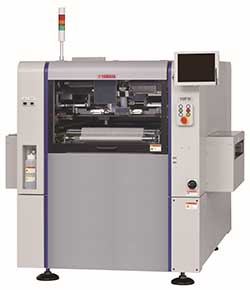
High-speed solder printing capability:
- 10* sec/cycle
- 12* sec/cycle including cleaning.
- Standard printing: under optimum condition, including board transfer time and printing time.
- Wet print accuracy: ±25 μm (6σ)
- Positioning repeat-ability accuracy: ±10 μm (6σ)
- Stencils up to L 750 x W 750 mm
- Printing head information:
- 3S head (3S = Swing Single Squeeze)
- Squeegee speed: 2 to 200 mm/sec
- Squeegee pressing force: 5 to 200 N +/- 2N (feedback control)
- Squeegee variable printing attack angle: 45 to 65 degrees
- Squeegee blade material: Metal or Urethane
- Options:
- 2D print inspection camera
- right-to-left transport
- PCB vacuum system
- UPS system
- PSC system (PSC: Print Stability Control)
- Temperature control unit
- Solder remaining quantity
- Automatic stencil exchange
- Automatic push-up pin exchange function
- Automatic solder transfer function
- Applicable PCB: L 610 x W 510 mm
- Software: YAMAHA Factory Tools
- Machine size: with conveyor: L 1.640 mm x W 1.990 mm x H 1.525 mm
- Machine weigh: 1.700 kg
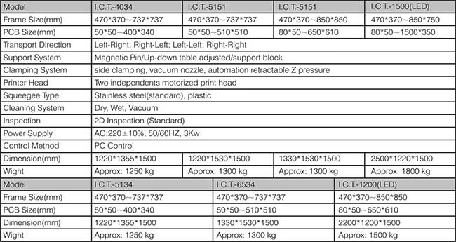
2. I.C.T-4034 Fully Automatic SMT Stencil Printer – I.C.T-4034 is a high precision automatic solder paste printer, correspond to industrial 4.0 and MES system. Through a higher level of automation, achieve zero defect.
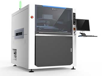
- High positional accuracy, repeated positioning accuracy ±0.01mm; printing accuracy 0.025mm
- Support glue printing, Automatic control improves production efficiency, quality control and saves production cost
- Automatic PCB calibration, Squeegee pressure adjustable, Automatic printing, Automatic stencil cleaning
- Programmable motor controls separation speed and distance among squeegee, stencil and substrate, to realize multi-method separation.
- Multi-functional PCB positioning system for convenient and accurate PCB positioning.
- Programmable PCB lifting platform ensure the PCB to lift to a proper height
- Adopt company independently developed suspended print head with automatic pressure adjustment system. Support on-line real time pressure feedback and automatic squeegee pressure balancing. Accurate pressure control ensures perfect paste forming effect.
Juki RV-2-3DHL(AOI/SPI)
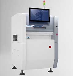
3D solder paste inspection machine (SPI)
3D board visual inspection machine (AOI)
Overwhelming speed
Remarkable accuracy
Features
• Overwhelming speed Large improvement in inspection tact with high-pixel (12 million pixels)
• Remarkable accuracy Using high-resolution lenses improves inspection accuracy of ultra compact components
• Ease of use of rating Process modes that are easy to use and create,from beginners to senior citizens
• Visual inspection automation RV series, which can also be used for measurement
• For improving the efficiency of the entire plant Achieving the efficiency of the entire factory through system linkage


