Objective
This lab activity uses the ADALM2000 and Scopy to introduce envelope detection and amplitude modulation. The signal’s envelope is equivalent to its outline, and an envelope detector connects all the peaks in this signal. Envelope detection has numerous applications in the fields of signal processing and communications, one of which is amplitude modulation (AM) detection.
AM is a modulation technique used in electronic communication, most commonly for transmitting information via a radio carrier wave. In AM, the amplitude (signal strength) of the carrier wave is varied in proportion to the waveform being transmitted. That waveform may, for instance, correspond to the sounds to be reproduced by a loud- speaker or the light intensity of television pixels.
A typical amplitude modulated signal can be seen in Equation 1.
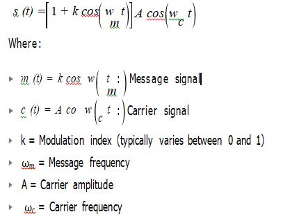
An envelope detector is an electronic circuit that takes a high frequency signal as input and provides an output, which is the envelope of the original signal (ωc » ωm).
It consists of two main elements:
▶ Diode/rectifier: Serves to enhance one half of the received signal over the other.
▶ Low-pass filter: Required to remove the high frequency elements that remain within the signal after detection/demodulation. The filter usually consists of a very simple RC network but in some cases it can be provided simply by relying on the limited frequency response of the circuitry following the rectifier.
Materials
- ADALM2000 Active Learning Module
- Solderless breadboard and jumper wire kit
- Two 1 kΩ resistors
- Two 1 μF capacitors
- Two 1N914 diodes
Envelope Detector
Background
Consider the circuit presented in Figure 1.

The capacitor in the circuit stores up charge on the rising edge and releases it slowly through the resistor when the signal falls. The diode in series rectifies the incoming signal, allowing current flow only when the positive input terminal is at a higher potential than the negative input terminal.

Hardware Setup
Build the breadboard circuit in Figure 2 for the envelope detector circuit.
Procedure
Use the first waveform generator as a source to provide the AM signal, with the following parameters:
- k = 0.5
- ωc = 10 kHz
- ωm = 100 Hz
- A = 3
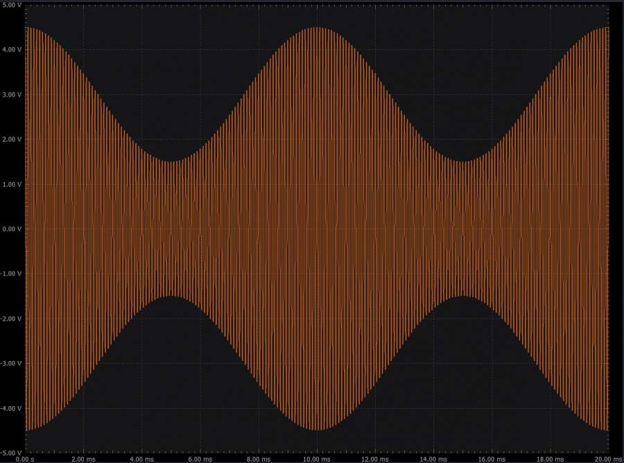
To generate the AM signal, use the math function from the Scopy signal generator. Set the record length to 20 ms, the sample rate to 75 MSPS, and apply the following function: (1 + 0.5 × cos (2 × pi × 100 × t)) × 3 × cos (2 × pi × 100 × 100 × t). The generated waveform is presented in Figure 3.
Configure the scope so that the output signal is displayed on Channel 1.
Disconnect the capacitor from the circuit and observe the output signal. A plot example is presented in Figure 4.
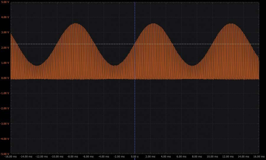
Without the capacitor connected, the circuit works like a positive half-wave rectifier that keeps the part of the signal that is above 0 V.
Now connect the capacitor back to the circuit. A plot example is presented in Figure 5.
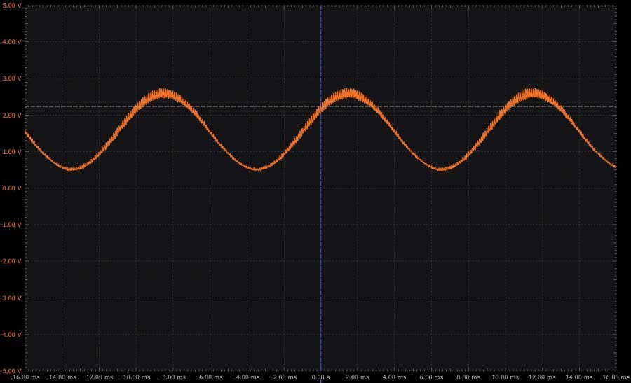
The obtained signal is the envelope of the positive half-wave obtained previously. It is actually the 100 Hz message signal with some 10 kHz variations on it (introduced by the carrier signal).
Frequency Domain Spectrum
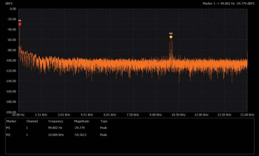
These signals can also be viewed in the frequency domain using the Spectrum Analyzer tool. First, look at the 10 kHz carrier and 100 Hz message signals together (since both are present at the output of this circuit). Enable Channel 1 and set the sweep range from 10 Hz to 15 kHz. Run a single sweep. Enable markers 1 and 2 from the Markers tab and the Marker Table. Move each marker using Prev Peak, Next Peak to set them on the carrier and the message signal. A plot example is presented in Figure 6.
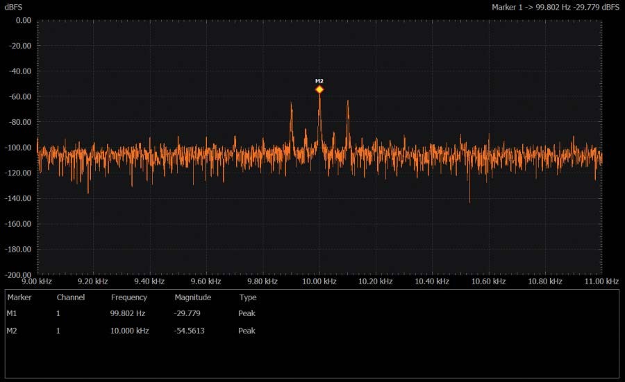
Set the sweep range from 9 kHz to 11 kHz. In Figure 7, the main peak is at the 10 kHz carrier frequency and there are modulation sidebands ±100 Hz on either side of the carrier (9900 Hz and 10100 Hz).
Set the sweep range from 20 Hz to 180 Hz. In Figure 8, the main peak is at the 100 Hz message frequency.
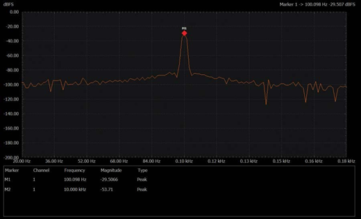
Since the frequency analysis is made on the output signal using a basic envelope detector circuit, both the message and carrier signal are shown. In contrast to the applied input signal, where the carrier amplitude is larger than the message amplitude, notice that the spectrum analyzer plot notice has, in terms of mag- nitude, a message signal (100 Hz) that is emphasized with respect to the carrier signal (see Marker table).
Extended Envelope Detector
Background
Consider the circuit presented in Figure 9.
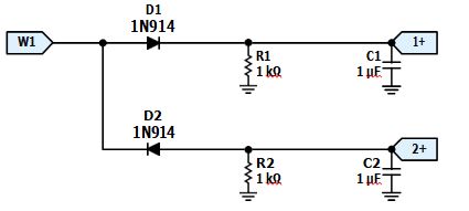
A similar circuit is added to the circuit in Figure 1. The only difference is that the diode is reversed, allowing the negative voltages to pass through the RC circuit.
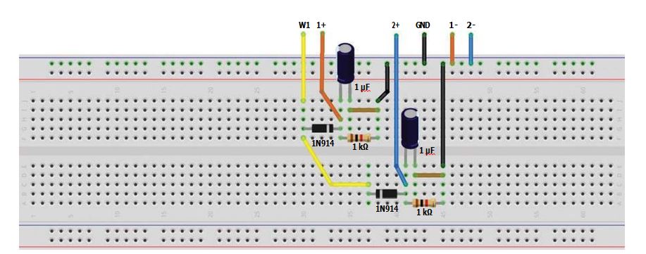
Hardware Setup
Build the breadboard circuit in Figure 10 for the extended envelope detector circuit.
Procedure
Use the first waveform generator as a source to provide the AM signal, with the following parameters:
- k = 0.5
- ωc = 10 kHz
- ωm = 100 Hz
- A = 3
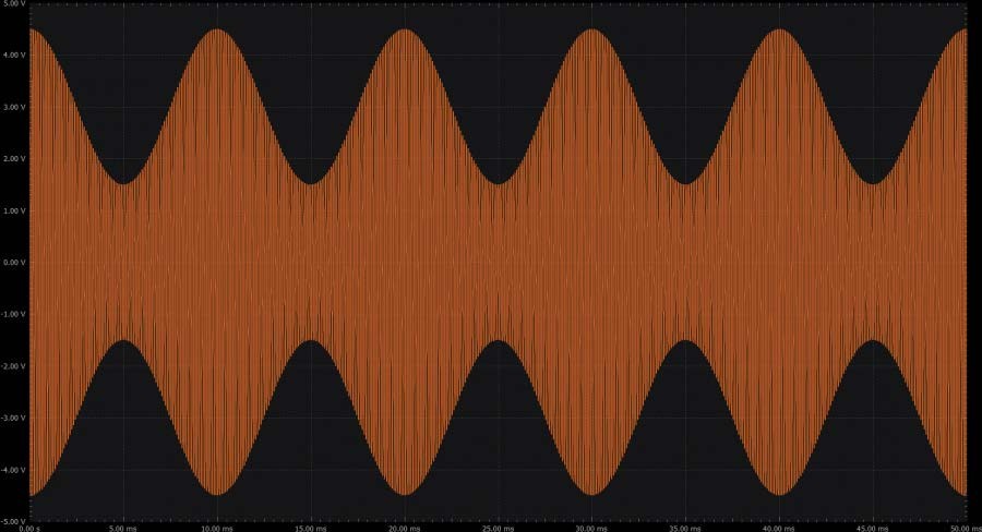
To generate the AM signal, use the math function from the Scopy signal genera- tor. Set the record length to 50 ms and apply the following function: (1 + 0.5 × cos (2 × pi × 100 × t)) × 3 × cos (2 × pi × 100 × 100 × t). The generated waveform is presented in Figure 11 (with five displayed periods).
Configure the scope so that the output signal is displayed on Channel 1.
Disconnect capacitors C1 and C2 from the circuit and observe the output signal. A plot example is presented in Figure 12.
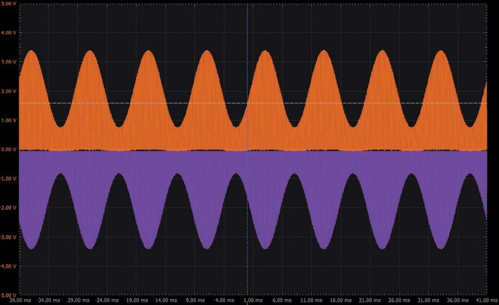
Without the capacitors connected, the circuit works like a positive half-wave rectifier and negative half-wave rectifier, separating the positive half from the negative one.
Now connect the capacitor back to the circuit. A plot example is presented in Figure 13.
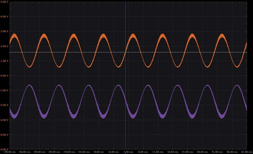
The obtained signal is the envelope of the positive half-wave and negative half- wave obtained previously.
Questions
- What happens if the capacitor/resistor values are changed? What are the draw- backs in this case?
- For the circuit in Figure 1, if a resistor is added in series with the diode, between D1 and R1, how is the output affected? Explain the differences.
Extra Activity: Biased Envelope Detector
The simple diode-based envelope detector of Figure 1 does not conduct well or at all if the amplitude—that is, the swing—is less than the forward turn voltage of the diode. It will suffer significant distortion on the negative half of the modulation signal for high modulation indexes (near 100%) when the diode is not fully turned on. A way around this limitation is to introduce a small DC bias to the diode. This small bias current moves to a quiescent operating point of the circuit to right at the turn on point of the diode.
Materials
- ADALM1000 Active Learning Module
- Solderless breadboard and jumper wire kit
- One 1.5 kΩ resistor (brown, green, red)
- One 10 kΩ resistor (brown, black, orange)
- One 20 kΩ resistor (red, black, orange)
- Two 1.0 μF capacitors (C1 and C2)
- One 2N3904 NPN transistor
- One 1N914 diode
Background
Consider the circuit shown in Figure 14
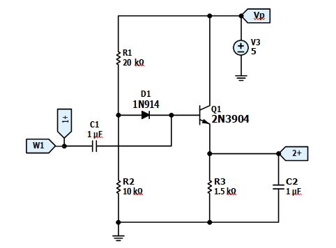
The amplitude modulated signal is AC-coupled into the base of NPN transistor Q1, which is configured as an emitter follower. Voltage divider R1 and R2 along with diode D1 act to set the DC bias point of the AC-coupled input (DC restoration). Absent any modulated input, the DC quiescent operating point seen at the emitter of Q1 will be the voltage at the junction of R1 and R2 minus the diode drop of D1 and the VBE of Q1. The base current of Q1 flows in diode D1 forward biasing it. During the positive half cycles of the modulated input, D1 turns off and the input signal peaks charge filter capacitor C2. During the negative half cycles of the input signal, transistor Q1 turns off and D1 conducts more strongly, supplying the input current.
Hardware Setup
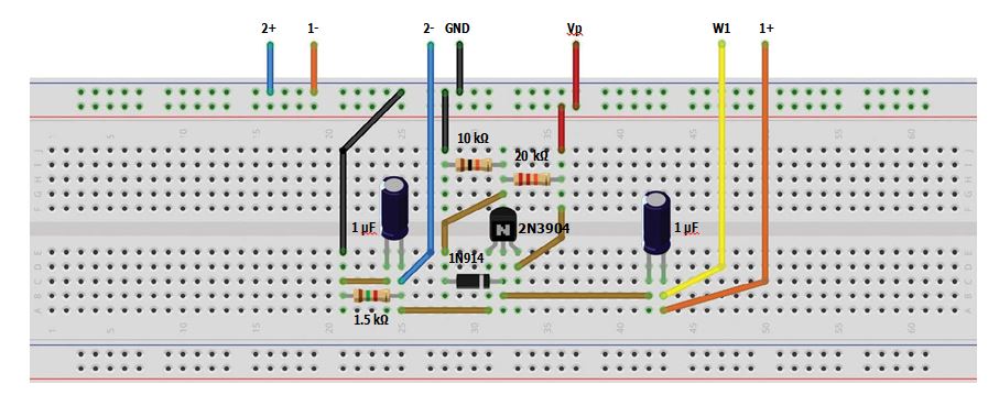
Build the breadboard circuit in Figure 15 for the biased envelope detector circuit.
Procedure
Connect the circuit to the 5 V supply.
To test this circuit, first use the same modulated signal used in the simple diode envelope detector example. Compare the new design to the simple diode enve- lope detector. Using the same steps as earlier, generate AM signals with smaller amplitudes/higher modulation indexes and compare the outputs of these two detector designs.
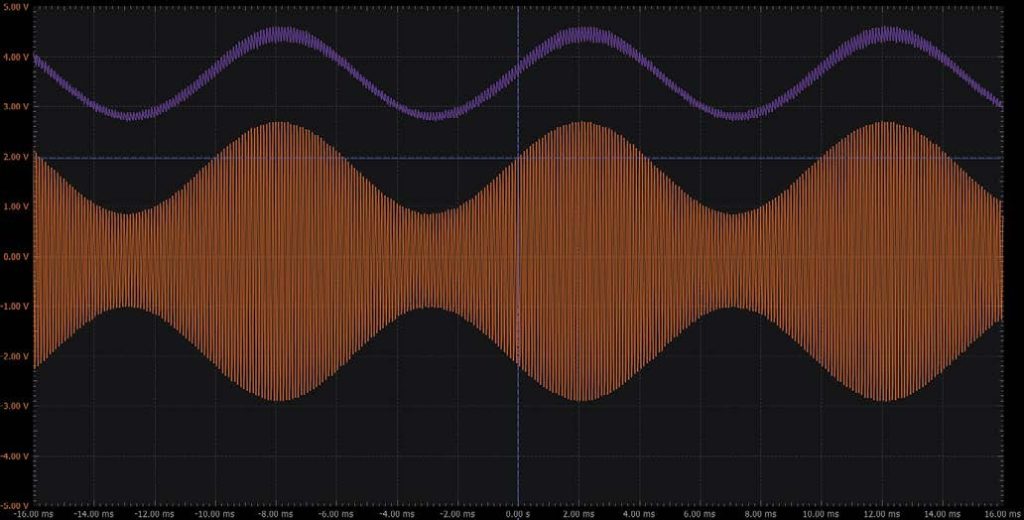
A plot example of the input and output waveforms for the biased envelope detector is presented in Figure 16.
Questions
- What are the basic components of an envelope detector circuit? Describe their role.
- How does the time constant (RC) of the envelope detector affect its performance?
You can find the answer at the StudentZone blog.
About the Author

Antoniu Miclaus is a software engineer at Analog Devices, where he works on embedded software for Linux and no-OS drivers, as well as ADI academic programs, QA automation, and process management. He started working at ADI in February 2017 in Cluj-Napoca, Romania. He holds an M.Sc. degree in software engineering from the Babes-Bolyai University and a B.Eng. degree in electronics and telecommunications from the Technical University of Cluj-Napoca.
About the Author

Doug Mercer received his B.S.E.E. degree from Rensselaer Polytechnic Institute (RPI) in 1977. Since joining Analog Devices in 1977, he has contributed directly or indirectly to more than 30 data converter products and holds 13 patents. He was appointed to the position of ADI Fellow in 1995. In 2009, he transitioned from full-time work and has continued consulting at ADI as a fellow emeritus contributing to the Active Learning Program. In 2016, he was named engineer in residence within the ECSE department at RPI.


