

The future of creating incredibly tiny, intricate structures is here, driven by a technology that marries digital precision with microscopic artistry: High-Resolution Digital Lithography (HRDL). This isn’t just an incremental improvement; it’s a paradigm shift, enabling unprecedented control over the micro and nano-world, opening doors to innovations once deemed impossible.
Beyond Silicon: The Expansive Reach of Ultra-Precise Patterning
While its roots are deep in semiconductor manufacturing, HRDL’s impact now ripples across diverse fields. Its core principle is deceptively simple: using focused light (often lasers or UV) or electron beams to directly “draw” patterns onto a light-sensitive material (photoresist) with exceptional precision, all guided by a digital blueprint. This direct-write approach eliminates the need for physical photomasks – the stencils of traditional photolithography – bringing unmatched flexibility and speed to the fabrication process.
The Engine of Precision: How HRDL Achieves the Unimaginable
What sets HRDL apart is its ability to achieve feature sizes measured in microns (µm) and even nanometers (nm) . This is made possible by several key technological advancements:
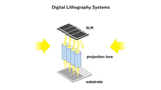
1. Advanced Spatial Light Modulators (SLMs) & DMDs: Imagine a microscopic array of millions of tiny mirrors (Digital Micromirror Devices – DMDs) or liquid crystal pixels. HRDL systems use these to dynamically shape and modulate the light beam with incredible fidelity, pixel-by-pixel, directly from a digital file. 2. Precision Optics & Focusing: Sophisticated lens systems focus the modulated light down to diffraction-limited spots. Advanced techniques like multi-photon absorption allow for even finer features by exploiting non-linear light-matter interactions, effectively beating the traditional diffraction barrier.
3. Stable Platforms & Metrology: Nanometer-scale patterning demands equally precise motion control. Ultra-stable stages and sophisticated real-time metrology systems ensure the substrate and the “drawing” tool are perfectly aligned and move with atomic-level accuracy.
4. Advanced Photoresists & Chemistry: Specially engineered photoresists react precisely to the intense, focused light or electron beams, enabling clean pattern development at the targeted high resolutions.
The Game-Changing Advantages: Why Industry is Embracing HRDL

The shift to HRDL offers compelling benefits over traditional methods:
- Unparalleled Flexibility & Rapid Prototyping: Change the design? Simply upload a new digital file. No costly, time-consuming mask fabrication needed. This accelerates R&D cycles dramatically.
- Maskless Manufacturing: Eliminates mask costs, storage, defects, and alignment issues, significantly reducing overhead, especially for low-volume, high-mix production.
- High Resolution & Accuracy: Consistently achieves features far smaller than the width of a human hair, enabling next-generation devices.
- Complexity Made Easy: Effortlessly creates intricate, non-repeating patterns, curved structures, gradients, and multi-layer alignments that are difficult or impossible with masks.
- Scalability & Cost-Effectiveness (for certain applications): While throughput can be a challenge for mass semiconductor production, HRDL excels in areas like prototyping, MEMS, photonics, and specialized devices where flexibility and precision outweigh sheer volume speed.
Where the Microscopic Meets the Revolutionary: Applications
HRDL is no longer just a lab curiosity; it’s actively shaping products and research:
Next-Gen Semiconductors: Prototyping advanced nodes, creating specialized test structures, fabricating photonic integrated circuits (PICs), and developing novel memory architectures.
- Advanced Micro-Electro-Mechanical Systems (MEMS): Manufacturing complex sensors, actuators, microfluidic channels, and bio-MEMS devices with intricate 3D features.
- Photonics & Optoelectronics: Fabricating waveguides, gratings, lenses (micro-optics), optical interconnects, and structured surfaces for enhanced light control.
- Flexible & Printed Electronics: Directly patterning conductive traces, electrodes, and components onto flexible substrates for displays, wearables, and sensors.
- Life Sciences & Medical Devices: Creating microfluidic “lab-on-a-chip” devices for diagnostics, patterning bio-compatible scaffolds for tissue engineering, and developing advanced biosensors.
- Security & Anti-Counterfeiting: Producing intricate optical security features like holograms and micro-text impossible to replicate conventionally.
The Future is Focused: Where HRDL is Headed
The trajectory of HRDL points towards even greater capabilities:
- Higher Throughput: Innovations in parallel writing (multi-beam systems) and faster modulation are closing the gap for higher-volume applications.
- Atomic-Scale Resolution: Pushing towards true atomic-level patterning using advanced electron beam and emerging techniques.
- Multi-Material & 3D Integration: Combining HRDL with other additive processes for true 3D microstructures incorporating diverse materials.
- AI-Driven Optimization: Using artificial intelligence to optimize patterning strategies, predict outcomes, and correct errors in real-time.
- Democratization of Fabrication: Becoming more accessible to universities and smaller companies, accelerating innovation beyond traditional semiconductor hubs.
Precision Unleashed
High-Resolution Digital Lithography is more than just a manufacturing tool; it’s an enabler of the microscopic revolution. By providing direct digital control over matter at scales invisible to the naked eye, HRDL is empowering scientists and engineers to build the next wave of technological marvels – from faster, smaller chips to life-saving medical devices and revolutionary optical systems. As the technology continues to evolve, pushing the boundaries of resolution, speed, and complexity, its impact will only grow, solidifying its role as a cornerstone of advanced manufacturing in the 21st century and beyond. The era of pixel-perfect micro-creation is well and truly underway.
References:1)chatGPT
About the author : I am B. E. in Industrial Production and served as lecturer in three different polytechnics for 10 years. I am also a freelance writer and cartoonist.