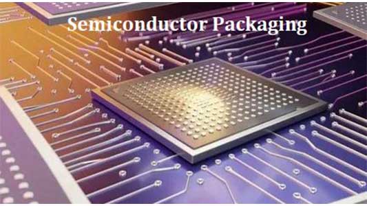
The unsung hero of the electronics world, semiconductor packaging, is stepping into the spotlight. As we move through 2025, it’s clear that the demand for more powerful, efficient, and compact chips isn’t slowing down. This push is directly fueling a revolution in how we package these tiny marvels of engineering. From powering the next generation of AI to making electric vehicles smarter, advanced packaging is the critical enabler.
Let’s dive into the top 10 trends that are defining the semiconductor packaging services market this year.

1. The Unstoppable Surge in Advanced Packaging
We’re moving beyond traditional methods. The market for advanced packaging is exploding, with projections pointing to massive growth, potentially exceeding $130 billion by 2034. Why? Simply put, Moore’s Law is getting harder and more expensive to maintain. Instead of just making transistors smaller, the industry is now focusing on packing them more intelligently within a package, leading to significant performance gains.

2. 3D and 2.5D Packaging Take Center Stage
Think of this as the era of “skyscrapers” for chips. 3D stacking and 2.5D interposer technologies are no longer niche; they are mainstream for high-performance applications. By stacking chips vertically (3D) or connecting them side-by-side on a silicon interposer (2.5D), we achieve incredible speeds and bandwidth while saving space. This is essential for AI accelerators, data centre servers, and high-end computing.
3. AI is Now Co-Designing the Package
Artificial Intelligence is infiltrating the packaging design process itself. Engineers are now using AI-driven tools to automate complex layout designs, predict potential thermal and mechanical stress points, and optimise the package for performance and yield. This results in fewer design iterations, a faster time-to-market, and more reliable final products.
4. The OSAT Ecosystem Continues to Expand
Very few semiconductor companies (fabless or IDM) want to manage the immense capital expenditure and specialised expertise required for cutting-edge packaging. This is why the Outsourced Semiconductor Assembly and Test (OSAT) sector is booming. The Outsourced Semiconductor Assembly and Test Market is estimated to grow at a CAGR of 3.6% during the forecast period 2024–2031, according to DataM Intelligence. Partnering with OSAT providers allows chip designers to leverage world-class packaging capabilities without the overhead, creating a more agile and efficient supply chain.
5. Flip-Chip Packaging Evolves for High-Speed Demands
Flip-chip technology, where the chip’s active area is facing down onto the substrate, has been around but is more relevant than ever. Its superior electrical performance, high-density interconnection capability, and excellent thermal management make it the go-to choice for 5G mmWave devices, high-speed networking gear, and GPUs.
6. Sustainability Becomes a Core Consideration
The electronics industry is facing increasing pressure to go green, and packaging is a major focus. We’re seeing a concerted shift towards researching and adopting sustainable materials—from greener moulding compounds to lead-free solders and recyclable substrates. Reducing the environmental footprint of packaging waste is no longer a “nice-to-have” but a business imperative.
7. Consumer Electronics Demand Pushes Miniaturisation
Our insatiable appetite for thinner, lighter, and more powerful gadgets is a primary driver of packaging innovation. Advanced packaging techniques like Fan-Out Wafer-Level Packaging (FO-WLP) are enabling the sleek designs of modern smartphones, wearables, and AR/VR glasses by integrating more functions into ever-smaller form factors.
8. Regional Diversification and Growth Hotspots
While the Asia-Pacific region, led by Taiwan, South Korea, and China, remains the dominant force in packaging manufacturing, interesting shifts are happening. Governments in other regions, including India, are making strategic moves. Initiatives like the planned ESDM (Electronics System Design and Manufacturing) parks in states like Uttar Pradesh signal a long-term goal to create a more geographically diverse and resilient supply chain.
9. Hybrid Bonding Emerges as a Key Enabler
Hybrid bonding is a game-changer for achieving ultra-fine interconnect pitch. This technique, which involves directly bonding copper pads without solder bumps, allows for dramatically higher density and performance between chips in a 3D stack. It’s becoming a critical technology for memory stacking and advanced heterogeneous integration.
10. Panel-Level Packaging Gains Traction for Scale
Why stop at round wafers? Panel-level packaging adapts processes used in the flat-panel display industry, using large, rectangular panels instead of traditional round wafers. This approach offers a significant increase in usable area, driving down costs especially for larger chips and is gaining strong interest for automotive and consumer electronics applications.
Conclusion: Packaging is the New Battleground
The message for 2025 is clear: the package is the product. The trends point towards an industry that is smarter, more sustainable, and deeply collaborative. Success in the semiconductor space will increasingly depend on mastering these advanced packaging technologies. For anyone involved in electronics design and manufacturing, keeping a close eye on these packaging innovations is no longer optional it’s essential.