Introduction
Oxygen saturation, electrocardiography, blood pressure, and respiration rate are measurements that used to be limited to hospital monitoring equipment. The monitoring of these parameters is key, especially for people at medical risk, either after an accident, after surgery, or when diagnosed with a serious disease. With an increase in an aging population and strong concerns with regards to overall health expenditures, access to medical monitoring outside of hospitals has become a growing trend. Now, at-risk patients are monitored during their day-to-day life in order to detect certain events earlier, or patients are being sent home from hospitals with monitoring devices to allow for a quicker, more comfortable recovery. There is a third group of users who are measuring these parameters for the purposes of prevention, even prior to any diagnoses.
Multiparameter monitors all share the same requirements: they need to be accurate, small, and operate for a long period of time from a single battery charge. To support this trend, a new family of single chip, biomedical analog front ends have been developed.
ADPD4000 Brief Overview
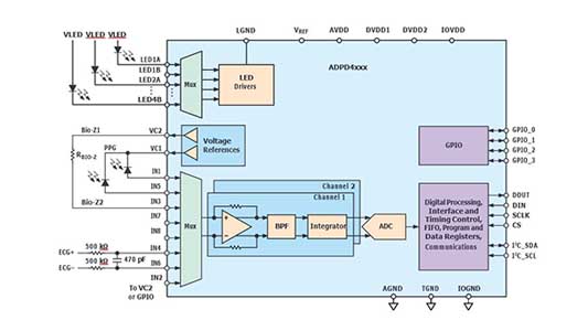
There are many multiparameter systems on the market that combine two or more measurements. Think of heart rate monitors combined with motion sensors to track activity, or heart rate variability with impedance sensing for applications like stress monitoring or sleep analyses. In most cases, each measurement is performed by a dedicated analog front end, resulting in several chips, each with its own analog-to-digital converter (ADC), its own interface to the main processor, and several power supplies and reference voltages that need to be decoupled. This results in many redundant building blocks, which is not an optimal system from a size and power point-of-view. In a wearable system, nothing is easier than having one main signal chain to which each sensor can be connected. The new ADPD4000 family of biomedical front ends is filling this gap in the market. Figure 1 shows a high level block diagram of the ADPD4xxx family. The front end is designed around two identical receive channels, which can be sampled simultaneously. Each channel is differentially built, which makes it possible to measure any sensor input in either a single-ended or differential measuring mode. The input stage is a transimpedance amplifier, with program- mable gain, followed by a band-pass filter and integrator, capable of integrating
7.5 pC per sample. The ADC is a 14-bit successive approximation register (SAR) converter having a maximum sampling rate of 1 MSPS. In front of each of the signal chains is an 8-channel multiplexer that gives the analog front end flexibility in routing the various sensor signals into the AFE.
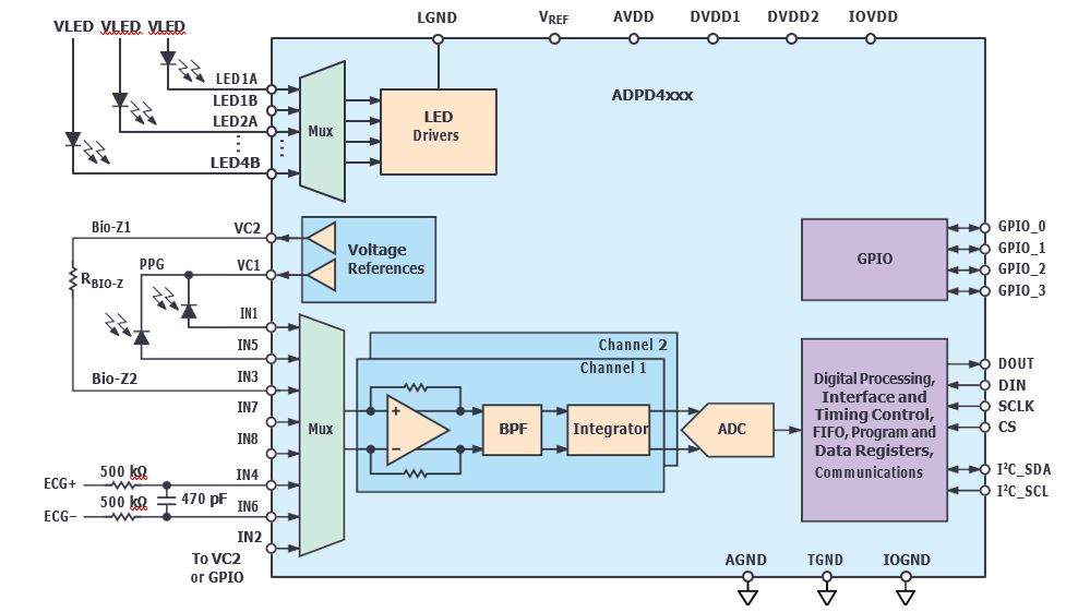
Various signals can be measured with this chip, as shown in Figure 1. You can modify the AFE as an optical front end, for instance, to measure either optical heart rate or oxygen saturation. In this mode, we measure photocurrent, and thus a high transimpedance input stage is needed to convert current into a voltage. We also need to cancel interference coming from ambient light. Another use case is when measuring biopotential signals from either electrocardiogram (ECG) or EMG sensors. This requires a different input signal chain setup, which requires reconfiguration of the front-end settings. Next to a receive signal chain, the chip also supports eight output drivers, which can be used to provide stimuli. You can configure one or more outputs to drive LEDs for an optical measurement, or one or more driver outputs can be used as excitation for impedance measurement either to measure skin impedance (electrodermal activity (EDA)) or electrode impedance—which affects the measurement quality—while performing a biopotential measurement.
The chip allows the user to preprogram each configuration or measurement in a certain time slot. It supports up to 12 time slots, which makes the system very easy to use once it is configured. Additionally, this chip does not require additional processor resources, which helps keep the system’s overall power consumption at a minimum. On the chip, you can oversample and average to improve the effective number of bits (ENOB) of the ADC. The decimated data path is 32 bits wide. Measurement results can be stored in a 256-byte or 512-byte deep FIFO (ADPD400x vs. ADPD410x).
There is a time stamp function integrated to support synchronization among data samples from several connected sensors. This is required once multiple sensor data are used to find correlation among the various measurement results. Figure 2 shows how this chip can be used to measure ECG synchronized to a photoplethysmography (PPG) measurement. Based on a pulse transit time (PPT) measurement technology, it is possible to measure blood pressure in a continuous mode. This is very attractive to people with hypertension. The time stamp function makes this possible.
Figure 3a shows how time slot operation can be supported. Each time slot starts with a precondition pulse, followed by a stimulus pulse, and finally, the photodiode current or signal from another sensor signal that is sampled by the ADC.
Figure 3b shows an example of an operation sequence. After power up, followed by a reset operation, the chip enters sleep mode. After waking up the chip, you can sequentially sample two ECG signals (for example, LEAD I and LEAD II), followed by an optical measurement to perform an SpO2 reading and an impedance measurement to measure skin conductance (EDA/stress). The process of attaining each of these measurements will be explained in the following section.
ECG Measurement Becomes So Much Easier
An ECG is the measurement of an electric signal generated by the human heart, due to depolarization and repolarization of the heart muscle per every heart beat. The signal is typically 0.5 mV to 4 mV in amplitude and measured over a frequency range from 0.05 Hz up to 40 Hz. An ECG can be performed to solely measure heart rate, but, in many use cases, we are more interested in the waveform itself, which can be used as a measure for cardiac performance or a prewarning to a potential cardiac event like arterial fibrillation or continuous hypertension. We can monitor cardiac activity by attaching electrodes to the skin. To guarantee good body contact in diagnostic applications, wet electrodes are typically used. The most popular are silver/silver-chloride (Ag/AgCl) electrodes. In out-of-hospital applications, these electrodes are very uncomfortable and can easily dry out or start to irritate the skin. Furthermore, though dry electrodes are often used, the contact between skin and electrode is degraded and dry electrodes are more sensitive to motion artifacts, resulting in a less than accurate read.
In an out-of-hospital (outpatient) application, there is always a trade-off between good quality electrodes and comfort. The ADPD4000 family can solve for this while also providing an accurate measurement despite electrode quality. Instead of using a voltage input, the ECG circuit measures electrical charge accumulated on a sensing capacitor. With an optimized time-constant calculated from the passive RC network and sampling rate, the charging process eliminates the variation on the skin-to-electrode contact impedance. Figure 1 shows how an ECG signal is coupled into the chip by an RC network. This ECG circuit has inherent immunity to variations in the skin-to-electrode contact impedance.
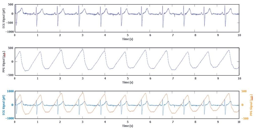
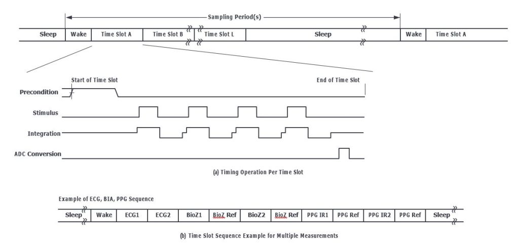
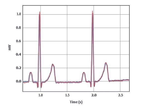
Figure 4 shows two ECG waveforms. The blue waveform has been measured with a good quality electrode, having a series impedance of 51 kΩ and 47 nF capacitance. The red waveform, though, is measured with a poor quality electrode, with high series impedance. It has a 510 kΩ contact impedance with 4.7 nF capacitance. We can see that the ADPD4000 is measuring both waveforms, almost identically, independent of the electrode quality. This is a huge advantage of this front end over alternative solutions on the market. An additional advantage is that this circuit is extremely power efficient since it doesn’t have to be active while capturing the ECG signal on the charge capacitor. Another advantage is that it consumes 150 µW to 200 µW.
PPG and Bioimpedance Measurement
For optical and bioimpedance measurements, LED drivers are required to emit light and to excite a current into the body, respectively. In many optical systems, more than just one wavelength is used, which makes this chip’s versatility highly desirable. The ADPD4000 has eight output drivers, where four channels can be used simultaneously with a programmable output current of maximum 200 mA per channel or 400 mA for the total driver section. Depending on the configuration, you can operate multiple time slots, each with its own wavelengths to measure,
for instance, optical heart rate, SpO2, hydration, or dehydration. Each receive signal chain has a programmable transimpedance amplifier followed by a dual-stage rejection block to cancel out ambient light interferers. The signal- to-noise ratio (SNR) of the transmit/receive signal chain is up to 100 dB for the ADPD41xx family, which makes it extremely useful for noise-sensitive optical measurements such as oxygen saturation measurement or blood pressure estimation. The power consumption of the optical system very much depends on the system configuration such as sampling and decimation rate, and the LED current used. This is also proportional to the location on the body and the skin tone of the user.
Many wearable systems can also measure skin conductance for applications like EDA, stress, or mental-state monitoring. An excitation current is needed in order to measure a voltage drop. The ADPD4000-family supports this use case. You can configure the chip in a 2- or 4-wire measuring mode. An enhanced waveform generator and DFT engine are not included, so in case impedance spectroscopy is required, the AD5940 should be used as a companion chip to complement the ADPD4000. The impedance function also can be used to measure electrode quality or for lead-off detection.
Since the ADPD4xxx has an 8-channel multiplexer, auxiliary inputs can also be sup- ported to measure either voltage, capacitance, temperature, or motion in a system.
Almost Ideal
With the introduction of the ADPD4000/ADPD4001, many of the challenges designers face when working on wearable devices, body patches, or drug delivery systems have been solved. For each of these use cases, performance, size, and power dissipation are critical specifications. This new biomedical front end, with its high performance, dual-channel sensor input stage, stimuli channels, digital processing engine, and timing control, meets all these require- ments. The ADPD4000 and ADPD4001 have reached volume production and are currently available, while the next generation, ADPD4100/ADPD4101, is expected to become available in the first quarter of 2020. This new generation has improved signal-to-noise specifications and additional features that can help to further reduce the power consumption of the entire system. Despite all these functions included in a single chip, it won’t make the electronic design engineer’s job redundant, as there are many parameters to configure to give each system its own identity.
About the Author
Jan-Hein Broeders is the healthcare business development manager for Analog Devices in EMEA. He works closely with the healthcare industry to translate their present and future requirements into solutions based on Analog Devices’ market-leading linear and data converter technol- ogy, as well as products for digital signal processing and power. Jan-Hein started in the semiconductor industry more than 25 years ago as a field applications engineer and has been in his current healthcare role since 2008. He holds a bachelor’s degree in electrical engineering from the University of ‘s-Hertogenbosch, the Netherlands. He can be reached at jan.broeders@analog.com.


