Introduction
From the beginning, one of the biggest challenge to radio designers has been the limitations of bandwidth. Early on, our radio forefathers thought that frequencies above a few hundred kHz were of no value because of detector limitations. Pioneers like Branly, Fessenden, Marconi, and many others struggled with this, until Armstrong and Levy perfected heterodyn- ing, opening higher frequencies of spectrum by downconverting to lower frequencies that detectors could adequately process with technology of the day. While higher frequencies were opened by the super-heterodyning process, the bandwidth was still relatively limited.
Until recent years, processing more than a few 10s of MHz has been a challenge and often limited to expensive solutions that often employed massively paralleled radio technology. It has long been desirable to simplify this and employ a method to simultaneously process as much bandwidth as possible. This capability has slowly evolved over the last few decades, as semiconductor processes and monolithic analog-to-digital converter (ADC) architectures have matured. From modest beginnings in the early ’90s until today, the direct RF sampling capability of ADCs has increased from about 20 MHz of Nyquist bandwidth, to over 5 GHz with products like the AD9213.
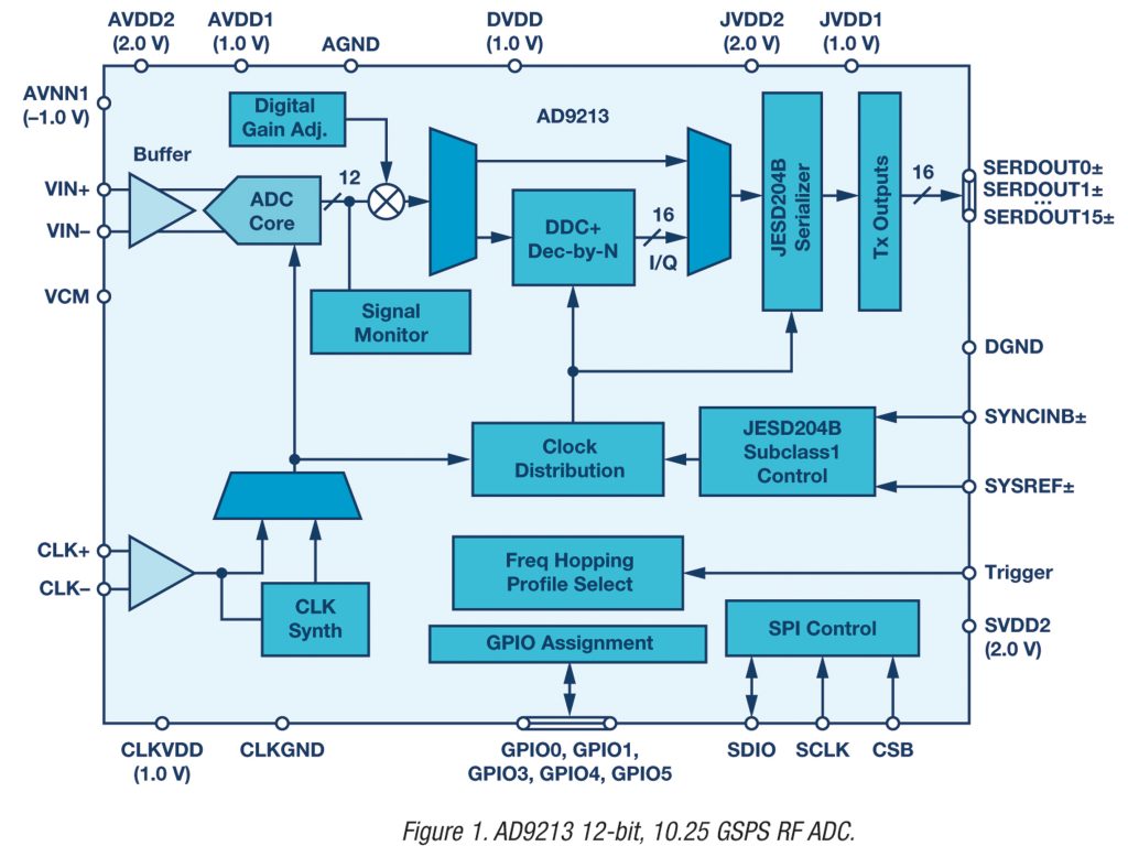
With the introduction of the AD9213 and the large instantaneous band- width it supports, many new options are opened, not just for instrument- grade receivers, but also for direct RF sampling radios, SIGINT, and radar.
Typical GSPS ADCs pose a unique challenge to overall performance, because they are constructed from multiple ADCs cores that are run in parallel to boost the net sample rate. Each of these converters must be
carefully timed and aligned and, even so, small errors between the con- stituent converters generate numerous spectral artifacts.1,2,3 Additionally, ADCs must accurately track the analog input signals and carefully sample and digitize them to prevent normal linear distortion. These two challenges, interleaving and raw bandwidth, make design of wide bandwidth ADCs very challenging where high fidelity is required, as in spectral applications like advanced radio and instrumentation.
The AD9213 is up to the challenge because of the excellent linearity under all signal conditions that is achieved by the implementation of on-chip dithering and calibration, yielding both higher frequency operations and performance. With a CW input at 4 GHz, the NSD is about –152 dBFS/Hz and SFDR is typically better than 65 dBc, including second and third har- monics. This enables true 5G instrument-grade receiver performance.
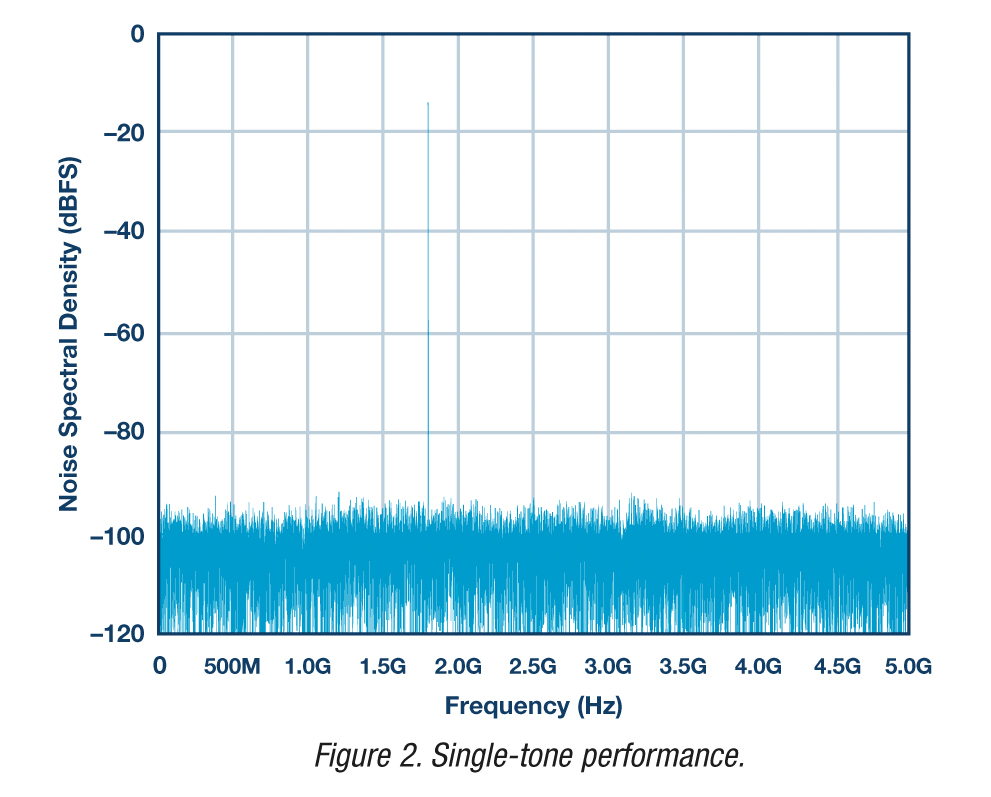
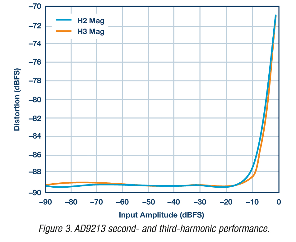
In addition to excellent high frequency performance, the behavior of low- order harmonics follows closely to what would be expected from a linear device. That is, harmonics behave as would be predicted by a simple poly- nomial, which is atypical for an ADC.4 This is important because it ensures high performance in both large signal and small signal environments.
As shown in the power sweep data of Figure 3, the second and third harmonics follow the predicted response based on their input level and once the noise floor of the measurement is achieved, there are no addi- tional recurrences at lower input levels. This is important because it allows these dominant spurs to be placed out-of-band when selecting a frequency plan. Spurious products of fourth-order and above are not significant. In heterodyning, radios mixer spurs must be carefully planned to avoid interference; the same is true for direct RF sampling.
Where Direct RF Sampling Wins
RF sampling is an interesting alternative to other radio architectures. Historically, data converter power has been very high to achieve levels of performance suitable for radio design. Previous studies have shown that for low cost, low power solutions, zero-IF radio architectures like the AD9371 always come to the top. This is evident in that all production cell phones, Bluetooth®, and similar devices have migrated to this architecture over the years for good reason. These are constrained bandwidth systems, but not necessarily constrained performance. For systems that require an arbitrarily narrow bandwidth, the zero-IF architecture is almost always the right solution. However, in applications where arbitrarily wide bandwidth is required, as in instrumentation, radar, and wideband communications, direct RF sampling has long been the goal. In these applications, it is understood that some of the cost and power efficiency afforded by other architectures is traded off for wider system bandwidth.
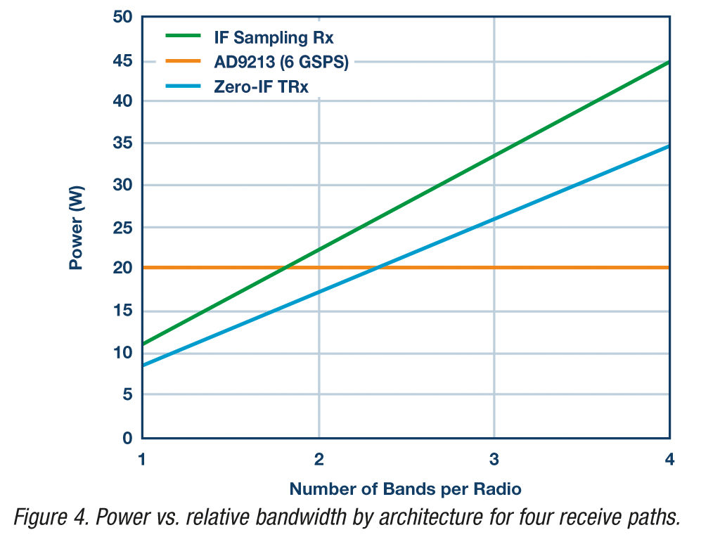
Therefore, when an RF sampling architecture is chosen, it is designed to cover the widest possible bandwidth to ensure overall radio performance. New RF ADCs like the AD9213 are designed to provide ultrafast sample rates beyond 10 GSPS and sample bandwidths more than 8 GHz, enabling direct RF sampling for many applications. Most radio services are allocated less than 75 MHz per band. With a 10 GSPS ADC, the effective utilization of spectrum is less than 2% of the Nyquist bandwidth. In several studies, the power efficiency of direct RF sampling is about 1/2 that of a zero-IF architecture. To improve overall efficiency in radio applications, RF sampling offers the possibility of sampling more than one band at a time.
As shown in Figure 4, for lower bandwidth requirements, traditional archi- tectures like IF sampling and zero-IF are much lower power than direct RF sampling. Only when you approach a bandwidth approximately 2× the latest bandwidth for zero-IF or IF sampling solution power does direct RF sampling make sense. Another way to look at this is that compared with a zero-IF or IF sampling solution, for constrained bandwidth systems, a direct RF sampling architecture will dissipate ≥2× the power of any other solution and cost about twice as much.
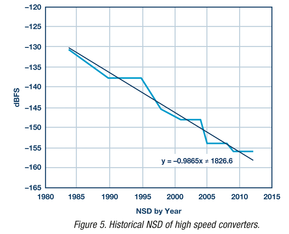
Over the last three decades, the noise spectral density (NSD) improvement has been about 1 dB per year, as measured from commercial devices and slightly better from academically graded papers.5 During this period, the focus was on ac performance, including bandwidth and SNR/harmon- ics. However, in the last few years, performance of converters has reached the point where they are good enough for most applications, and now the focus has begun shifting from ac performance to power dissipation and silicon area (cost).
In Figure 6, sample rate is plotted on the horizontal axis with figure of merit on the vertical axis. Over time, faster converters are developed. Devices that fall near the technology front at a given point in time tend to be cutting edge in terms of sample rate and historically are higher in power and lower figure of merit (FOM). Once the technology front has passed a given sample rate, newer devices at that rate show improved figure of merit, which translates into lower power, smaller die size, and reduced cost moving toward the architectural front. According to Murmann’s latest data set, the AD9213 is just inside the technology front indicating that future converters in this class will exhibit lower power and the other benefits.
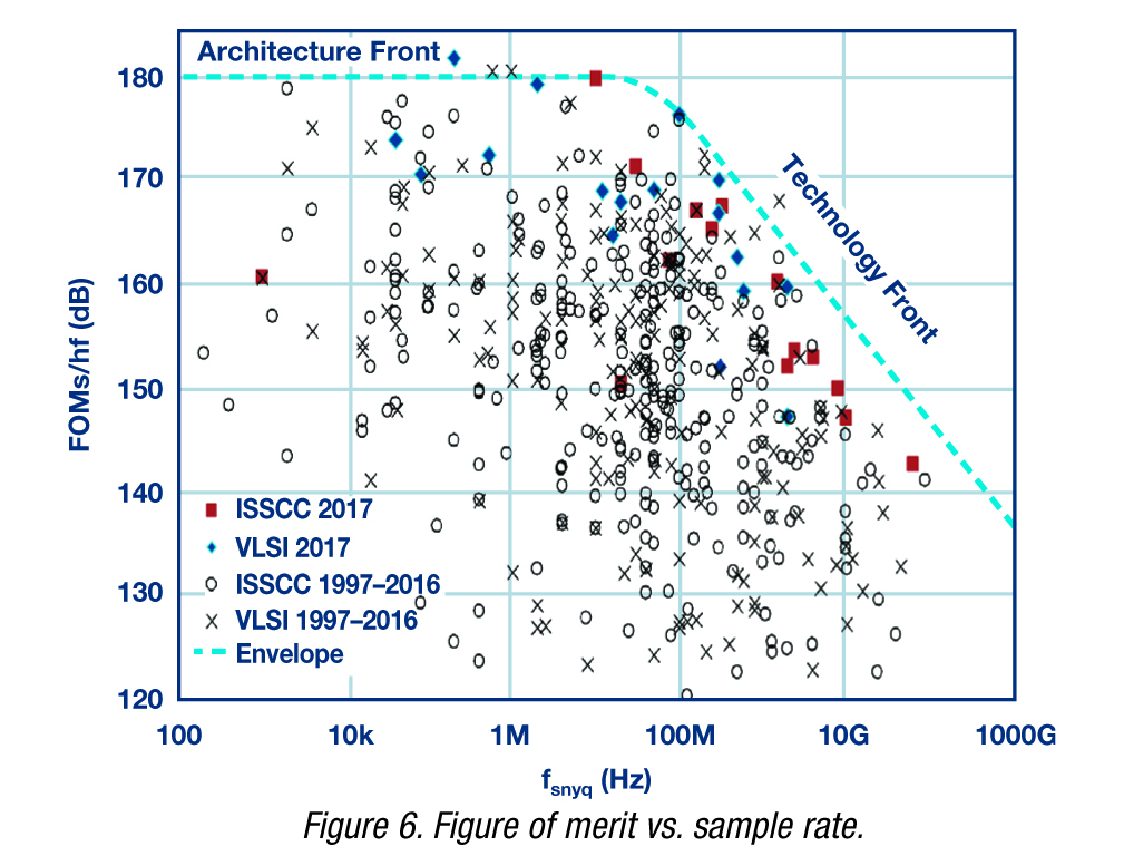
This trend creates an interesting shift. RF power in the front end is domi- nated by physics, which is moving power from the antenna connector to the ADC input and, thus, isn’t elastic in the way that Moore’s law indicates for digital functionality. Thus, as converter power continues to fall over the next few generations, the dominant power contributor will become the amplifiers and their dissipation will remain approximately flat where it is today rendering the contribution from the ADC, including the interface much less a contributor and in decline.
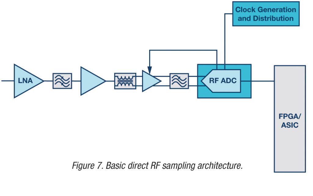
Figure 7 shows a basic direct RF sampling architecture consisting of a string of amplifiers and appropriate filtering. As expected, there are
no frequency translation stages, only amplifiers used to increase the signal levels required to overcome noise within the ADC itself and broad RF filters to prevent undesired aliasing within the converter itself.
As for filtering, two approaches are possible. First, the widest filter possible could be applied, taking care to prevent aliasing. Typically, it is possible to create a broadband filter that provides up to 80% of Nyquist and could cover first or second Nyquist zones with good performance. In most cases it wouldn’t be reasonable to have a passband that crosses Nyquist zones because of aliasing, but there are cases where this is appropriate in well- defined situations.
A second approach to filtering is to provide two or more pass bands for the ADC. A key advantage of a GSPS ADC is that the high sample rate facilitates very flexible frequency planning and placement of the analog signals. In the case of multiband radios, typical RF SAW filters can be configured on separate RF amplifiers to process each band separately and then summed into the ADC for sampling. It is possible that each of these bands could fall into separate Nyquist zones if they do not alias onto the same frequency. Having separate amplifiers for each band allows gain to be optimized for each band, which minimizes crossband desensitization and maximizing performance. However, as noted earlier, the RF power can be significant and other options exist for multiband.
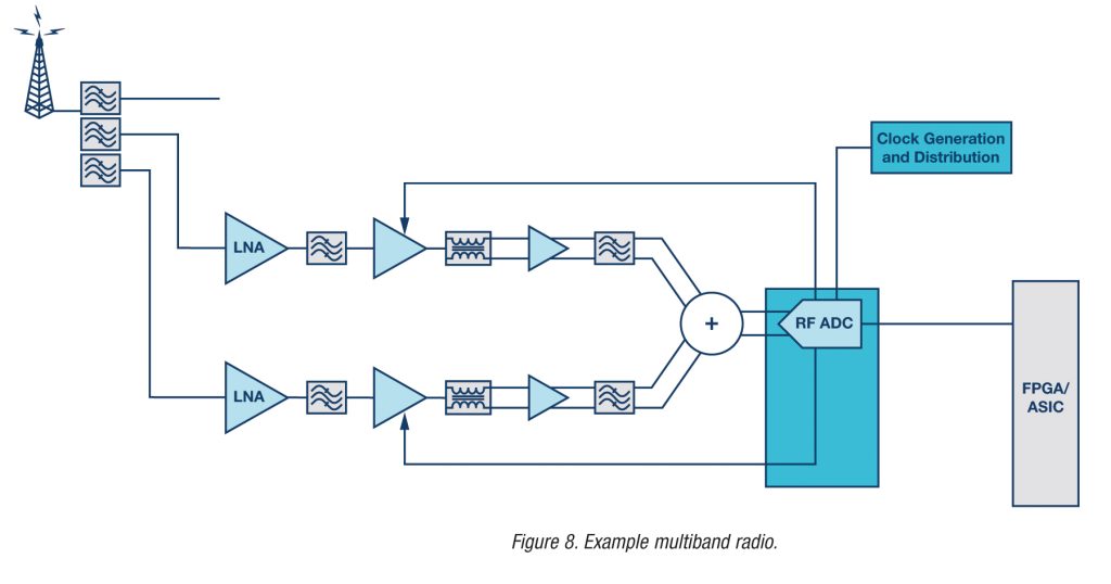
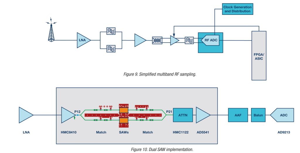
In some cases, several bands can be separately filtered but amplified by way of a single RF amplifier chain. This has the advantage that power in the RF chain is optimized by sharing a single gain path. However, perfor- mance between the two bands must be somehow traded off. This means that if one band has a large signal that requires gain to be adjusted, it will impact the performance on the other band. In many cases, this is accept- able given the relative dynamic ranges required. One such implementation is in Figure 9. While this application focused on cell phone bands, it is easily adapted to other applications including wideband instrumentation, such as spectrum analysis and sampling scopes.
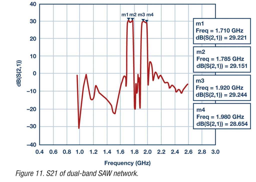
A specific implementation of this is shown in Figure 10. For this design, the input and output matching networks to SAW filters were carefully designed to ensure that, at the resonance of one band, the network on the other side appeared as an open circuit. It should be noted that the matching network included lumped elements, as well as transmission lines. In that manner, the interaction between the two different circuit paths was minimized.
By careful design, it is possible to get quite good performance from these networks. The forward transmission characteristics are shown in Figure 11. Here, the characteristics of each individual SAW filter is preserved without impacting the other. In this design, Band 1 and Band 3 are parallel. Other bands or frequency ranges could have been chosen and the method will still work.
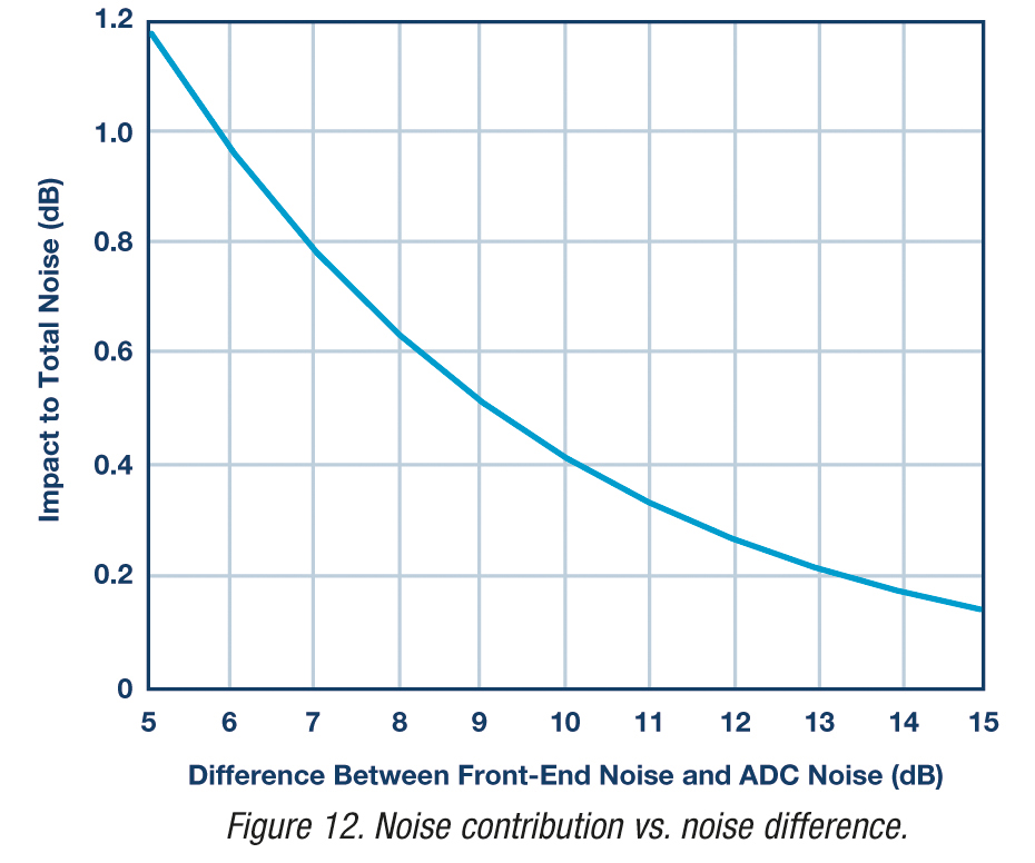
As for signal level planning, several issues should be kept in mind. When designing with ADCs, one of the first rules to follow is to apply enough gain in front of the ADC that front-end noise swamps out that of the ADC. While ADCs continue to improve, the noise from an ADC is not Gaussian in nature and can cause many issues in the performance of any system that includes them.4 Figure 12 shows the relationship between the difference in the front-end noise referred to the ADC input, the ADC noise, and the resulting impact on overall noise. A general guideline is to keep front-end noise more than 10 dB above that of the ADC. If followed, this would ensure that the ADC would only contribute less than 0.4 dB to the total noise. This ensures that the system performance will follow expectations.
From the AD9213 data sheet, the typical NSD is about –152 dBFS/Hz. With a nominal full-scale of 7 dBm, this represents –145 dBm/Hz. Front-end thermal noise should target –135 dBm/Hz representing a gain plus NF of at least 39 dB. As built in Figure 10, the circuit provided a gain of 43 dB and a NF of 3 dB increasing total front-end noise to –128 dBm/Hz. Under no input conditions, the difference between the two is about 19 dB for maxi- mum gain. As the input signal is increased, the ADC noise floor increases a few dB due to the jitter of the clock source used.
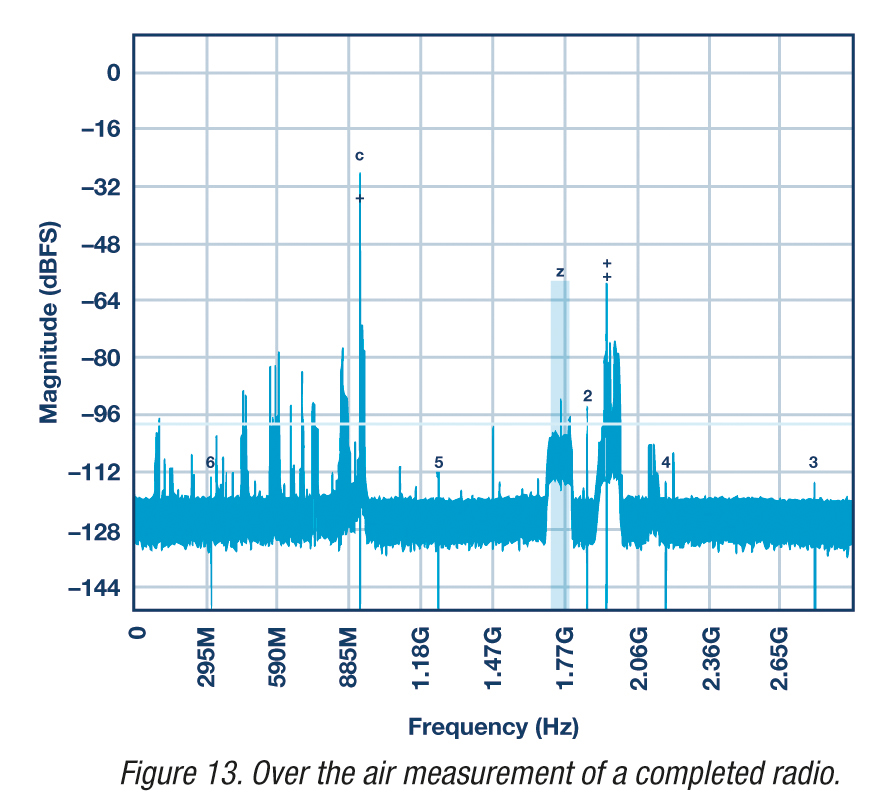
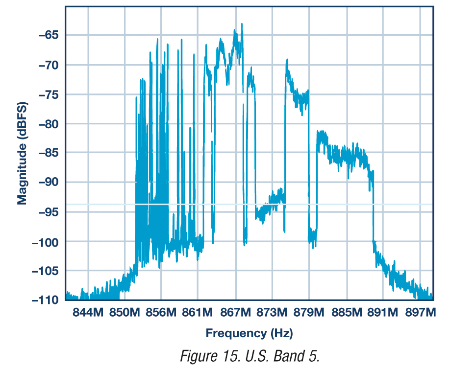
Figure 13 provides an example of an over air measurement of a completed radio. Because this is a very broadband radio with more than 2 GHz of bandwidth with minimal filtering, many signals are visible. The left half of the spectrum shows frequencies up to about 900 MHz including high power FM and television broadcasts. Above this, minimal frequencies are seen until the pass band of the two SAW filters covering 2.1 GHz (UMTS Band 1) and 1.8 GHz (UMTS Band 3). Band 3 is identified by the shading but both bands show an elevation of the noise floor as anticipated by the excess front-end noise passing through the filters. Since these measurements were made in the U.S., very little is detected in Band 3, but Band 1 captures part of the down link of Band 2. Above this, the anti-alias filter removes any remaining signals and the noise floor is quiet.
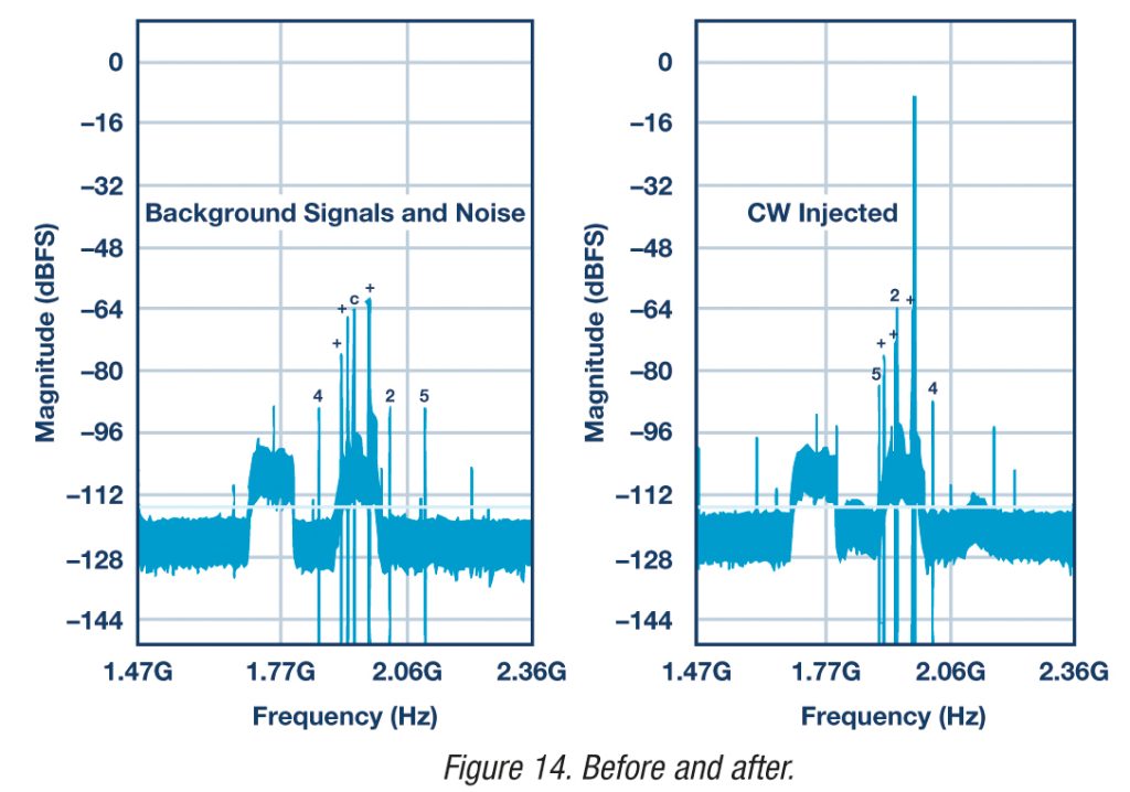
Zooming in on the two bands covered by the parallel SAW filters gives a little more detail. Figure 14 shows a side by side comparison of background noise on the left and injection of a near full-scale CW signal on the right. Looking at the wideband noise floor and not the two pass bands, you can see that the noise floor comes up slightly on the right when the large CW signal is injected. This is due to jitter on the clock convolving with the analog input.6 Now comparing the noise floors of the two pass bands, no increase is detected in the noise floor within the two pass bands. This is because the thermal noise from the front-end swamps out the ADC noise floor increase when a large signal is applied. If you look closely at the raw data you can see an increase of about 0.3 dB in the noise floor in the pass band, which corresponds to an 11 dB difference in the noise accord- ing to Figure 12.
Conclusion
While heterodyning radios of various types continue to dominate designs, wideband ADC technology has matured to the point where RF sampling is possible for a wide range of applications once dominated by frequency translating designs. As shown in this article, new options exist for direct sampling wideband systems. Products like the AD9213 introduce the possibility of high fidelity digitization well above 2 GHz, making it an ideal candidate for applications that require large instantaneous bandwidths including scopes, analyzers, and wideband/multiband radios. While some have said this was not possible for GHz RF frequencies, the AD9213 has pushed through those barriers and future generations show the promise continued improvements. Converter products continue to evolve and mature in ways that continue to push the boundary of performance and efficiency, making them an ideal candidate for GHz wideband systems.
References
- Gabriele Manganaro and David H. Robertson. “Interleaving ADCs: Unraveling Mysteries.” Analog Dialogue, Vol. 49, 2015.
- Jonathan Harris. “The ABCs of Interleaved ADCs.” EDN Network, 2013.
- Jonathan Harris. “Further into the Alphabet with Interleaved ADCs.” EDN Network, 2013.
- Brad Bannon. Application Note AN-410: Aperture Uncertainty and ADC System Performance. Analog Devices, Inc., 1995.
- B. Murmann, “ADC Performance Survey 1997-2016,” [Online]. Available: http://web.stanford.edu/~murmann/adcsurvey.html.
- Brad Brannon and Alan Barlow. Application Note AN-501: Aperture Uncertainty and ADC System Performance. Analog Devices, Inc., 2006.
About the Authors
Brad Brannon has worked at ADI for 32 years, following his grad- uation from North Carolina State University. At ADI he has held positions in design, test applications, and system engineering. Brad has authored a number of articles and application notes on topics that span clocking data converters, designing radios, and testing ADCs. Currently, Brad is responsible for system engineering for 4G and 5G receive architectures. He can be reached at brad.brannon@analog.com.
Steve Dorn has more than 35 years of experience working with microwave and RF products. He joined the Wireless Systems Group of ADI in 2016. Previously, he worked at Skyworks, RFMD, Maury Microwave, and Motorola where he gained experience with design verification, PA load pulling, RF probing, RF PCB design, and product characterization. He can be reached at steve.dorn@analog.com.
Vandita Pai Raikar is a systems engineer working in the Wireless Systems Group, Communications Business Unit at Analog Devices, Inc. She is actively involved in the development of 4G/5G communication platforms—specifically RF/microwave antennas and component designs based on industry trends and customer dialog. She pos- sesses a master’s in electrical engineering with a focus on RF/ electromagnetism. She has a background in RF engineering and antenna design. She can be reached at vandita.raikar@analog.com.
The authors would like to thank Kenny Man for developing the hardware for this project. Without his contribution, this article would not be possible.


