Electronics Era

  • About Us
  • Advertise with Us
  • Contact Us
  • e-Mag
  • Webinars
Header logo on website
Advertisement
Advertisement
Menu
  • News
    • Industry News
    • Product News
  • TECH ROOM
    • Sensor
    • VR / AR
    • Embedded
    • Medical Electronics
    • Industry 4.0
    • Robotic
    • Automation
    • Smart Machine
    • Component
    • Manufacturing
    • Aerospace & Defence
    • Security
    • Policy
  • Semiconductor
    • AUTOMOTIVE ELECTRONICS
      • EVs
      • HEVs
      • ADAS
      • Connected Cars
    • IoT-Internet of Things
      • Development Kit
      • IoT Design
    • Power Electronics
      • AC-DC/DC-DC Converters
      • Mosfets
      • IGBTs
      • LEDs
  • T & M
    • 5G testing
    • Oscilloscopes
    • SDN & NFV
    • RF & Wireless
  • AI/ML
  • Telecom
    • 5G/6G
  • RENEWABLES
    • Sustainability
  • Future Tech
    • Data Center
    • Cloud Computing
    • Big Data Analytics
  • Webinars
  • Editor’s Pick
    • Tech Article
    • Tech Blog
    • White Papers
    • EE-Tech Talk
    • Market Research
  • EE Awards
    • EE Awards 2025
    • EE Awards 2024
  • MORE
    • E-Mag
    • Events
    • Subscription
    • Contact Us
Home News Industry News

KeenSemi Signed a MoU with VLSI Expert Pvt Ltd

Editorial by Editorial
November 7, 2024
in Industry News
Reading Time: 3 mins read
KeenSemi Signed a MoU with VLSI Expert Pvt Ltd
Share on FacebookShare on TwitterShare on LinkedIn

Delhi– KeenSemi, a leading semiconductor design consultancy, faces one of the industry’s most pressing challenges: the shortage of skilled technical talent. With the global demand for advanced systems in AI, IoT, and high-performance computing, the need for specialized professionals has reached unprecedented levels.

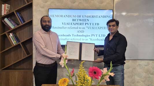
To address the talent gap more strategically, KeenSemi has signed a Memorandum of Understanding (MoU) with VLSI Expert Pvt. Ltd., a leading technical training institute specializing in semiconductor design training. This collaboration aims to equip aspiring engineers with industry-relevant skills through intensive training modules focused on key areas of ASIC design.

Semiconductor design requires deep technical expertise and foresight into future technology trends. As more countries, including India, prioritize building local semiconductor ecosystems, the demand for skilled engineers far outweighs the supply, creating a significant talent gap across the industry. By creating a pipeline of skilled professionals, KeenSemi ensures a steady influx of capable talent, directly addressing industry needs and fostering a future-ready workforce to support the company’s growth and the development of India’s semiconductor ecosystem.

According to Mr. Pankaj Panjwani, CEO & Founder of KeenSemi, the shortage of talent is a critical challenge for both established firms and startups. “The global semiconductor industry is expanding rapidly, but there is a notable gap in the availability of professionals with a holistic understanding of the semiconductor product life cycle. This shortage is particularly acute in areas like physical design, physical verification and reliability, design-for-test, advanced node implementation methodologies, and post-tapeout bring-up,” said Mr. Panjwani.

With semiconductor chips embedded in everything from consumer electronics to automotive systems, the need for robust chip design is paramount. The industry’s move towards advanced fabrication nodes (1.8nm, 3nm, 5nm) has increased the demand for engineers proficient in cutting-edge technologies.

KeenSemi, known for its innovative solutions in communication, automotive, IoT, and high-performance computing sectors, is playing a key role in the design and development of India’s first ARM Neoverse-based high-performance compute solution, “Aum.” The “Aum” System-on-Chip will place India among the few nations with their own high-performance computing solutions.

KeenSemi emphasizes upskilling its workforce, with leadership actively mentoring engineers to meet the technical demands of modern chip design. The company also collaborates with external institutes to train and hire promising junior engineers, building a future-ready workforce capable of tackling the industry’s complex challenges. Leveraging cutting-edge Electronic Design Automation (EDA) tools, KeenSemi streamlines chip design processes, allowing engineers of all experience levels to contribute meaningfully to projects.

Looking ahead, Mr. Panjwani remains confident in KeenSemi’s ability to address the talent shortage and continue leading innovation. “Our multi-pronged approach ensures that we remain competitive while expanding capabilities to meet the demands of both domestic and international markets,” he stated.

KeenSemi is committed to contributing to India’s growing semiconductor ecosystem by playing a pivotal role in the development of indigenously designed products and solutions, aligning with the broader goal of making India a global leader in semiconductor design and manufacturing.

Tags: KeenSemisemiconductorsemiconductor designVLSI
Editorial

Editorial

Join Our Newsletter

* indicates required
Electronics Era

Electronics Era, India's no.1 growing B2B news forum on Electronics and Cutting Edge Technology is exploring the editorial opportunity for organizations working in the Electronics Manufacturing Services(EMS) Industry.

Follow Us

Browse by Category

  • 5G testing
  • 5G/6G
  • AC-DC/DC-DC Converters
  • ADAS
  • Aerospace & Defence
  • AI/ML
  • Automation
  • AUTOMOTIVE ELECTRONICS
  • Big Data Analytics
  • Blockchain
  • Cloud Computing
  • Component
  • Connected Cars
  • Data Center
  • Editor's Desk
  • EE-Tech Talk
  • Electronics Components
  • Embedded
  • EVs
  • Future Tech
  • HEVs
  • Industry 4.0
  • Industry News
  • IoT-Internet of Things
  • LED & Lighting
  • LEDs
  • Manufacturing
  • Market Research
  • Medical Electronics
  • Mosfets
  • News
  • Oscilloscopes
  • Policy
  • Power Electronics
  • Product News
  • RENEWABLES
  • RF & Wireless
  • Robotic
  • SDN & NFV
  • Security
  • Semiconductor
  • Sensor
  • Smart Machine
  • SMT/PCB/EMS
  • Sustainability
  • T & M
  • Tech Article
  • Tech Blog
  • TECH ROOM
  • Telecom
  • Uncategorized
  • VR / AR
  • White Papers

Recent News

Lam Research

First of Its Kind: Dextro Cobot Wins Best of Sensors Award for Revolutionizing Fab Maintenance

June 27, 2025
DC-DC-Power-Converter

Microchip Expands its Space Portfolio with the SA15-28 DC-DC Power Converter and Companion SF100-28 EMI Filter

June 27, 2025
  • About Us
  • Advertise with Us
  • Contact Us

© 2022-23 TechZone Print Media | All Rights Reserved

No Result
View All Result
  • News
    • Industry News
    • Product News
  • TECH ROOM
    • Sensor
    • VR / AR
    • Embedded
    • Medical Electronics
    • Industry 4.0
    • Robotic
    • Automation
    • Smart Machine
    • Component
    • Manufacturing
    • Aerospace & Defence
    • Security
    • Policy
  • Semiconductor
    • AUTOMOTIVE ELECTRONICS
      • EVs
      • HEVs
      • ADAS
      • Connected Cars
    • IoT-Internet of Things
      • Development Kit
      • IoT Design
    • Power Electronics
      • AC-DC/DC-DC Converters
      • Mosfets
      • IGBTs
      • LEDs
  • T & M
    • 5G testing
    • Oscilloscopes
    • SDN & NFV
    • RF & Wireless
  • AI/ML
  • Telecom
    • 5G/6G
  • RENEWABLES
    • Sustainability
  • Future Tech
    • Data Center
    • Cloud Computing
    • Big Data Analytics
  • Webinars
  • Editor’s Pick
    • Tech Article
    • Tech Blog
    • White Papers
    • EE-Tech Talk
    • Market Research
  • EE Awards
    • EE Awards 2025
    • EE Awards 2024
  • MORE
    • E-Mag
    • Events
    • Subscription
    • Contact Us

© 2022-23 TechZone Print Media | All Rights Reserved

Advertisement
Advertisement