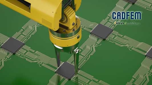
In today’s high-tech world, IC packaging is not just a functional necessity but a strategic enabler of innovation in electronics and semiconductors. It bridges the gap between cutting-edge chips and real-world applications, ensuring reliability, performance, and scalability. As the demand for compact, high-speed, and energy-efficient devices grows, IC packaging technologies must address increasingly complex challenges.
Simulation technologies have become indispensable in overcoming these challenges. With leaders like TSMC, Intel, and Samsung driving advancements, and simulation tools like Ansys enabling precision design, the semiconductor industry is pushing boundaries.

This article explores the latest advancements in IC packaging, key simulations, and how emerging trends and Ansys solutions are shaping the future of electronics.
Advancements in IC Packaging Technologies
1. TSMC’s 3DFabric™ Technology
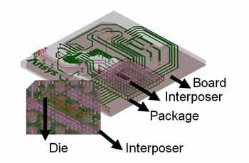
TSMC’s 3DFabric™ is a pioneering platform that integrates 2D, 2.5D, and 3D IC packaging technologies. It enables vertical stacking of silicon dies (3D packaging) and horizontal placement of heterogeneous components on silicon interposers (2.5D packaging). These techniques deliver superior performance, lower power consumption, and higher integration density.
The 3DFabric™ Alliance further accelerates innovation by offering ecosystem collaboration for design, memory modules, substrates, testing, and manufacturing. This comprehensive support simplifies adoption and reduces time to market.
2. Intel’s Packaging Innovations
Intel is redefining IC packaging with advanced technologies like Foveros (3D stacking) and EMIB (Embedded Multi-die Interconnect Bridge). These approaches enable heterogeneous integration of high-performance components. Intel’s vision to achieve 1 trillion transistors per package by 2030 reflects their leadership in advanced packaging.
3. Samsung’s Focus on 2.5D and 3D ICs
Samsung is advancing Redistribution Layer (RDL) technologies to support high-performance computing and IoT applications. By enhancing interconnect density and improving routing flexibility, Samsung’s packaging solutions enable miniaturized designs without compromising performance.
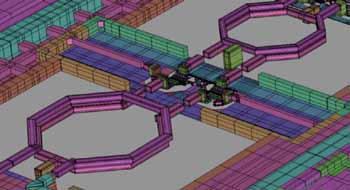
Key Simulations for IC Packaging
Simulation tools streamline the design process, enabling faster iterations and validation. CADFEM, as an Ansys Elite Channel Partner, provides tailored solutions and support for engineers to leverage tools like HFSS, SIwave, and Q3D Extractor, ensuring robust IC packaging designs from the early stages.
1. Chip-Package-System Co-Simulation
Modern IC packaging requires a holistic approach to simulate the interactions between the chip, package, and system. Co-simulations ensure that the entire ecosystem works seamlessly, minimizing issues such as impedance mismatches, thermal hot spots, and signal degradation.
2. Electromagnetic Simulation of IC Designs
High-frequency designs operating at GHz and mmWave frequencies demand precise electromagnetic simulations. These simulations evaluate parasitics, coupling, and signal propagation to ensure robust performance in RF and high-speed digital applications.
3. Manufacturability and Design for Yield (DFY)
Simulations now extend beyond electrical performance to address manufacturability concerns. Design for Yield (DFY) simulations evaluate process variations and manufacturing constraints to ensure high-quality production with minimal defects.
4. Coupling and Multiphysics Effects
The increasing complexity of IC packaging introduces coupling effects between electrical, thermal, and mechanical domains. Multiphysics simulations analyze these interactions to optimize designs holistically, ensuring performance, reliability, and longevity.
5. Early Design Stage Insights
Simulations at the early design stage enable engineers to detect and resolve potential issues before physical prototyping. This approach reduces development cycles and avoids costly redesigns, fostering a “first-time-right” design philosophy.
6. Faster Time to Market
Simulation tools streamline the design process, enabling faster iterations and validation. By reducing design and testing cycles, companies can bring products to market quickly, gaining a competitive edge.
Emerging Trends in IC Packaging
1. Heterogeneous Integration
Combining diverse components—such as processors, memory, and accelerators—into a single package is becoming standard in high-performance applications. Simulations ensure seamless integration, optimized interconnects, and robust power delivery for these complex systems.
2. 2.5D and 3D Packaging Technologies
The shift to 2.5D and 3D packaging enhances performance while reducing form factor. However, these designs introduce challenges like interconnect parasitics, signal integrity, and heat dissipation, all of which require sophisticated simulation tools.
3. RF and mmWave Integration
5G and IoT applications demand IC packages that support high-frequency signals with minimal loss. Advanced simulations ensure impedance matching, low insertion loss, and compliance with electromagnetic interference (EMI) standards.
4. AI-Driven Design Optimization
Artificial intelligence (AI) is transforming the IC packaging landscape by enabling predictive analytics and automated optimization. AI-powered tools accelerate design cycles and improve decision-making during simulations.
5. First-Time-Right Designs

The push for first-time-right designs is reshaping how engineers approach IC packaging. With advanced simulation tools, potential issues are addressed upfront, eliminating expensive design iterations and ensuring reliability.
How Ansys Drives Innovation in IC Packaging
Ansys tools, supported by partners like CADFEM, empower engineers to address complex challenges in IC packaging, ensuring performance, reliability, and manufacturability. CADFEM offers training, implementation support, and expertise to maximize the impact of Ansys solutions in real-world applications. Here’s how Ansys empowers engineers to achieve innovation:
1. Ansys HFSS-IC
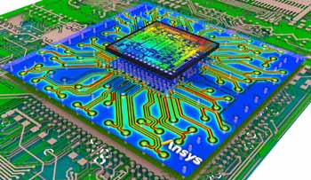
HFSS-IC™ is a specialized solution for 3D electromagnetic simulation of integrated circuits. Its ability to model high-frequency interconnects, parasitics, and coupling effects ensures optimal signal and power integrity in complex designs.
2. Ansys HFSS
HFSS provides full-wave electromagnetic simulations for RF, mmWave, and high-speed digital applications. It’s a powerful tool for designing antennas, interconnects, and components that comply with EMI/EMC standards.
3. Ansys SIwave
SIwave specializes in signal and power integrity analysis for IC packages and PCBs. It enables decoupling capacitor optimization, PDN analysis, and crosstalk evaluation, ensuring robust performance in high-speed designs.
4. Ansys Q3D Extractor
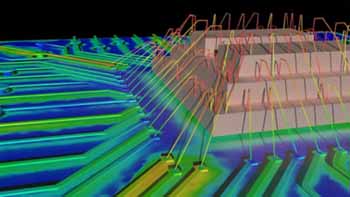
Q3D Extractor provides precise parasitic extraction for dense IC layouts, ensuring engineers can identify and mitigate parasitics that impact performance.
5. Ansys RedHawk-SC
For chip-level power integrity and reliability analysis, RedHawk-SC offers industry-leading capabilities. It ensures robust power delivery for advanced nodes and evaluates reliability under varying operating conditions.
6. Integrated Multiphysics Simulations
Ansys tools enable co-simulation across electromagnetic, thermal, and mechanical domains, addressing the growing need for multiphysics analysis in advanced packaging.
7. Early-Stage Simulation and Manufacturability
Ansys provides tools that allow engineers to simulate designs early in the process, identifying potential issues before they escalate. DFY tools ensure that designs are manufacturable, reducing production risks and increasing yield.
Conclusion: Pioneering the Future of IC Packagin
As the semiconductor industry advances, IC packaging is playing a central role in enabling next-generation devices. Technologies like TSMC’s 3DFabric™, Intel’s Foveros and EMIB, and Samsung’s RDL are pushing the boundaries of performance and miniaturization.
Simulation is the cornerstone of this progress, ensuring designs are optimized for performance, reliability, and manufacturability. Ansys tools such as HFSS-IC, SIwave, and Q3D Extractor empower engineers to address the complexities of modern IC packaging, enabling first-time-right designs and faster time to market.
By embracing advanced simulations and staying ahead of emerging trends, organizations can unlock the full potential of IC packaging. With trusted partners like CADFEM, companies can seamlessly adopt Ansys tools and methodologies, ensuring they stay competitive and innovate effectively in the rapidly evolving electronics and semiconductor industries.
About The Author:
Satish is a Technology Specialist in Electronics and Semiconductors at CADFEM India, a leading provider of simulation-based engineering solutions. With a focus on delivering cutting-edge expertise in simulation-driven design, Satish specializes in providing electronic systems and semiconductor technologies across diverse industries.
At CADFEM India, an Elite Channel Partner of Ansys in engineering innovation, the emphasis lies on empowering businesses through simulation technology. From electronics and semiconductors to fluid mechanics and structural analysis, CADFEM India delivers solutions that enable faster product development, enhanced performance, and cost optimization. For enquiries contact [email protected], 9849998435.