How a wide-bandgap upstart is redefining radar, electronic warfare, secure comms, and directed energy—while resetting the SWaP-C baseline for military systems.
Introduction

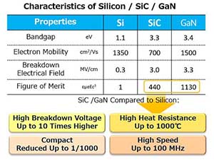
Gallium nitride (GaN) has moved from promising lab curiosity to the default choice for high-power, high-frequency RF and power-conversion hardware at the heart of modern defense systems. With a wide bandgap (~3.4 eV), high critical electric field, strong electron saturation velocity, and excellent thermal robustness—especially when grown on silicon carbide (SiC)—GaN devices deliver more RF output power per millimeter, higher efficiency, and better survivability than legacy gallium arsenide (GaAs) and silicon (Si) technologies. The result is clear, measurable advantage across active electronically scanned array (AESA) radars, electronic attack and protection suites, beyond-line-of-sight and SATCOM terminals, space and missile seekers, and the power stages that feed directed-energy payloads.
This cover story lays out the physics that make GaN different, the device and packaging innovations that translate materials performance into fielded capability, and the system-level implications—particularly size, weight, power, and cost (SWaP-C). We also look at reliability maturation, thermal management, digital linearization, and supply-chain realities, then close with a playbook for program managers and architects deploying GaN at scale.

Why GaN? The Physics That Matter
Three intrinsic properties explain GaN’s defense relevance:

- High breakdown field: GaN’s critical electric field is an order of magnitude higher than Si and several times that of GaAs. Practically, that allows higher drain voltages and, therefore, higher load impedances and power densities for RF power amplifiers (PAs). Designers can use fewer output devices and smaller passive networks to reach the same wattage—directly shrinking the transmit/receive (T/R) module footprint.
- High electron velocity and 2DEG formation: AlGaN/GaN heterostructures form a polarization-induced two-dimensional electron gas (2DEG) with very high sheet carrier density. High electron velocity at microwave and millimeter-wave frequencies preserves gain at X-, Ku-, and Ka-bands and pushes usable bandwidth higher with less efficiency penalty.
- Thermal resilience: GaN-on-SiC stacks leverage SiC’s high thermal conductivity to draw heat away from hot spots. Combined with GaN’s wide bandgap, the devices tolerate junction temperatures that would rapidly degrade GaAs or LDMOS. That translates to higher duty cycles, more robust survival in electronic attack environments, and fewer thermal constraints on duty factor and pulse width.

Bottom line: For the same aperture and cooling capacity, GaN delivers more ERP/EIRP, more range, better jam resistance, and improved multi-mission agility.
From Wafer to Warfighter: Device Structures and Materials Choices
HEMTs, p-GaN HEMTs, and MIS-Gate Variants
Defense-grade GaN PAs rely on AlGaN/GaN high electron mobility transistors (HEMTs). Gate engineering is crucial:
- Schottky-gate HEMTs offer simplicity and low parasitics for high-frequency operation.
- p-GaN gate (enhancement-mode) devices simplify gate bias and can improve ruggedness for some power electronics roles.
- MIS-gated HEMTs use thin dielectrics for reduced gate leakage and improved reliability, though interface traps must be managed.
Substrates: GaN-on-SiC vs. GaN-on-Si (and GaN-on-Diamond)
- GaN-on-SiC is the workhorse for high-power RF. It balances thermal performance, lattice matching, and supply maturity.
- GaN-on-Si reduces substrate cost and die size for power electronics and some RF where ultimate power density is not required, and is attractive for very high-volume production.
- GaN-on-Diamond is emerging for extreme heat flux; diamond’s thermal conductivity can substantially lower channel temperature, unlocking even higher power density or improved reliability margins. It remains niche due to cost and manufacturability but is highly relevant for next-gen EW/RF payloads.
MMIC Integration
Monolithic microwave integrated circuits (MMICs) combine gain stages, power combining, bias networks, and sometimes limiters/detectors on a single die. For defense AESA, GaN MMICs in each T/R module move more RF power closer to the radiating element, cutting waveguide losses and enabling thinner, lighter panels.
Flagship Applications
- AESA Radar: Range, Resolution, and Duty Cycle
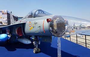
Active Electronically Scanned Array Radar (AESA) Radar on Tejas Aircraft (Image Courtest DRDO)
Impact: GaN PAs increase effective isotropic radiated power (EIRP), enabling longer detection ranges or smaller apertures for a given range. Higher back-off efficiency improves average power and duty cycle, which supports more agile waveforms—simultaneous multi-function radar (MFR), air/surface modes, and low-probability-of-intercept (LPI) operation.
Design notes:
- Power density: State-of-practice GaN MMICs deliver double-digit W/mm at X- and Ku-band with PAE often exceeding 50% at back-off in Doherty or load-modulated topologies.
- Linearity: Digital pre-distortion (DPD) and crest-factor reduction (CFR) borrowed from telecoms improve spectral containment and EIRP under modern radar waveforms (OFDM-like or multitone stress).
- Thermal: Microchannel cold plates, vapor chambers, and advanced thermal interfaces (e.g., diamond heat spreaders) maintain junction temperatures under high PRF and long pulse widths.
Operational payoff: Higher dwell-time and rapid beam steering (via AESA) provide better track quality and resilience against jamming. GaN’s robustness also increases tolerance to high VSWR conditions, important for naval radars subjected to icing, sea spray, or impact damage.
2) Electronic Warfare: Power, Bandwidth, and Survivability
Electronic attack (EA) requires broadband, high-power, and resilient transmitters that can survive reflections and high peak voltages. GaN shines here:
- Wideband PAs using non-uniform matching networks and distributed architectures deliver octave-spanning coverage with usable efficiency.
- Ruggedness against load mismatch and elevated case temperatures supports rapid retunes and “shoot-through-the-array” concepts.
- Instantaneous bandwidth supports cognitive/jamming techniques and reactive countermeasures. GaN helps maintain gain and phase linearity critical for coherent techniques such as DRFM-based deceptive jamming.
3) Secure SATCOM, Tactical Comms, and Datalinks
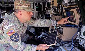
Image courtesy U.S. Army Program Executive Office Command, Control and Communications-Tactical (PEO C3T)
Modern tactical waveforms (e.g., high-order QAM with strong FEC) demand linearity and efficiency at back-off. GaN PAs in SATCOM and line-of-sight radios:
- Enable smaller terminals with higher EIRP for man-portable or UAV use.
- Maintain spectral masks under DPD, even at high average power.
- Support Ka-band terminals with aperture-integrated T/R modules, reducing feed losses and mechanical complexity.
A system-level nuance: The combination of GaN PAs and envelope tracking (ET) can preserve efficiency across the signal’s crest factor. ET requires fast, low-impedance DC/DC stages; GaN power FETs on the supply side are often used to implement these, creating a GaN-feeds-GaN virtuous cycle.
4) Missile Seekers and Proximity Fuzes
Space and volume are brutally constrained in missile seekers. GaN’s power density allows compact RF chains for active seekers at millimeter wave, improving target discrimination and resistance to countermeasures. Robustness to high G-loads (with suitable packaging) and temperature cycling is now proven in operational hardware.
5) Space Systems
Radiation effects are a perennial concern. GaN devices show inherent tolerance to total ionizing dose (TID) and single-event effects compared to many silicon processes, though mission assurance still demands thorough screening and guardbanding. GaN PAs and switches in space-based SAR, communications payloads, and crosslinks enable higher EIRP and reduced mass for deployable arrays.
6) Power Electronics for Directed Energy and Pulsed Power
GaN is not only an RF story. Enhancement-mode GaN power FETs and gate-injected transistors (GITs) provide:
- High-frequency switching for compact DC/DC converters feeding high-voltage Marx banks or capacitor chargers in directed-energy weapons (DEWs).
- Lower switching losses than silicon IGBTs or many Si-MOSFETs at comparable voltages, increasing efficiency and enabling lighter, quieter power supplies.
- Fast transient response crucial for pulse-forming networks and beam quality stabilization.
Packaging, Thermal, and Module-Level Engineering
From Die to T/R Module
To extract performance from GaN die, RF package and module design must manage parasitics, heat, and mechanical stress:
- Flange-mount and QFN-style packages use copper-molybdenum or copper-tungsten carriers to match coefficients of thermal expansion (CTE) and spread heat.
- Die-attach choices (eutectic AuSn, transient liquid phase sintering, or advanced solders) affect reliability at high junction temperatures and under thermal cycling.
- RF interconnects (wirebond vs. flip-chip) trade assembly complexity for parasitic control; at Ka-band and above, flip-chip and air-bridge strategies reduce inductance.
- Module integration combines PA, LNA, limiter, T/R switch, phase shifter, and vector modulator. GaN excels for high-power transmit; GaAs pHEMT or SiGe BiCMOS often remains preferred for ultra-low-noise receive chains, yielding heterogeneous modules.
Thermal Architectures
- Baseplate technologies: Copper diamond, pyrolytic graphite, and vapor chamber baseplates isothermally spread heat under dense arrays.
- Cold-plate optimization: Microchannels matched to module footprints reduce thermal resistance. CFD-driven design and digital twin models are now standard practice.
- Advanced TIMs: Indium-based foils, pressure-optimized elastomers, and solder TIMs reduce interface resistance; reliability under shock/vibration is validated to MIL standards.
Linearity, Efficiency, and Waveform Agility
GaN’s efficiency at high output power is a major draw, but modern defense waveforms push adjacent-channel leakage (ACLR/ACPR) and EVM requirements that force PAs to operate backed off from P_sat. Key techniques:
- Doherty and asymmetric Doherty architectures extend high efficiency into back-off region (6–10 dB), useful for multi-tone EA and complex comms waveforms.
- Digital pre-distortion (DPD) linearizes AM/AM and AM/PM distortion. Wideband DPD (hundreds of MHz) is challenging at Ka-band but increasingly practical with fast converters and FPGA/SoC platforms.
- Load-modulated balanced amplifiers (LMBA) and outphasing are active research areas for very wideband linearization.
Practical tip: Leave board-level hooks (couplers, observation receivers) in T/R modules for factory DPD characterization and in-theater recalibration.

Reliability: From Current Collapse to Mission Assurance
Early GaN faced trap-induced phenomena—current collapse, gate and drain lag, and dynamic R_on increases under RF drive. The industry has mitigated these through:
- Surface passivation and field-plate engineering to reduce surface traps and electric field crowding.
- Optimized buffer doping to limit leakage paths and dispersion.
- Gate metallurgy and dielectric stacks that limit hot-electron degradation.
Reliability qualification follows JEDEC- and MIL-style regimes adapted for GaN’s failure modes:
- HTOL and HTRB with RF stress rather than only DC.
- Thermal cycling and power-cycle testing at elevated ΔT_j to mimic radar/EW duty factors.
- VSWR survivability testing—both open/short and frequency-dependent mismatch—ensures ruggedness in the field.
Takeaway: Mature GaN MMICs now meet life requirements for air, sea, land, and space platforms when derated appropriately and cooled effectively.
System-Level Implications: SWaP-C and MOSA
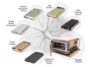
A typical CMOSS MFRF [multifunction, radio-frequency] system.]
SWaP-C Gains You Can Bank
- Smaller apertures for same range, or longer range for same aperture.
- Reduced thermal load for a given EIRP, cutting coolant flow and pump power.
- Lower part counts in PAs and matching networks, improving reliability and maintainability.
- Platform agility: Lighter AESA panels simplify gimbal mechanics (or enable fixed conformal arrays), enhancing survivability and cross-section control.
Modular Open Systems Approach (MOSA)
GaN’s performance pairs well with MOSA initiatives (e.g., SOSA/CMOSS) that define card-level electrical, thermal, and mechanical interfaces. Standardized power budgets and cooling envelopes make it easier to re-use GaN T/R modules across platforms. For maximum reuse:
- Adhere to common control planes (I²C/SPI) for bias and health reporting.
- Expose diagnostics (RF power, temperature, VSWR) via standard telemetry.
- Use field-replaceable module designs with blind-mate RF and coolant connectors.
Supply Chain, Export, and Trusted Foundry Considerations
GaN for defense intertwines with export controls and trusted manufacturing requirements. Program offices typically:
- Qualify multi-source second-sourcing for wafer and assembly to reduce risk.
- Maintain obsolescence management plans with last-time-buy triggers due to fast commercial cadence.
- Evaluate on-shore vs. off-shore processing tradeoffs, sometimes splitting epitaxy, wafer fabrication, and assembly across different trusted nodes.
For space and missile programs, lot screening (radiation, burn-in, and RF stress) is often tailored beyond catalog screening to ensure mission assurance.
Emerging Frontiers
- GaN-on-Diamond
Demonstrations show significant junction temperature reductions at the same RF power, enabling either higher PAE or increased power density. Expect first operational deployments where SWaP is brutal (high-bandwidth EA pods, hypersonic seekers). - Monolithic Integration with Passive/Front-End Functions
On-die integration of high-Q passives is improving; co-packaging GaN with SiGe/CMOS control ICs in System-in-Package (SiP) form reduces latency and harness count. - W-band and Beyond
For high-resolution imaging radar and data-links, advanced gate processes (≤ 100 nm) sustain gain at 75–110 GHz with meaningful power per element, unlocking compact millimeter-wave arrays. - Adaptive Thermal and AI-Assisted Control
Real-time health monitoring and AI-guided bias control adjust quiescent currents and back-off in response to aging and environment, maximizing field life without conservative derates. - Radiation-Hard Power GaN
As electrification of spacecraft grows, rad-tolerant GaN power FETs and drivers are enabling lighter, more efficient power systems for EP thrusters and high-throughput payloads.
Practical Design Playbook
Architecture & Waveform
- Co-design RF and waveform: Choose PA topology (Doherty, outphasing) with the intended radar/EW/comm waveform in mind to balance linearity and efficiency at the actual back-off.
- Leave headroom: GaN can deliver high peaks; budget EVM/ACLR and thermal margins for worst-case PAPR.
Thermal & Mechanical
- Start with T_j: Derive allowable junction temperature from reliability targets, then flow down to baseplate ΔT and coolant specs.
- Verify under mismatch: Test hot-soak + high VSWR across the band; include protective limiters and fast bias shutdown where needed.
Module Control & Monitoring
- Bias sequencing: Implement deterministic gate/drain sequencing to protect HEMTs.
- Health telemetry: Embed on-module sensors (temp, current, forward/reflected power); design for in-situ calibration and prognostics.
DPD/Calibration
- Observation paths: Add couplers and digitizers for DPD training; include temperature-aware models to keep linearity over the mission envelope.
- Factory vs. field: Pre-train models and permit quick in-field retraining to account for array-level coupling changes.
Verification & Qualification
- RF stress benches: Validate under representative duty cycles and pulse structures, not just CW.
- Radiation & environment: For space/missile, execute TID, SEE, and displacement damage tests and correlate to device physics models.
Program Manager’s Checklist
- Mission fit: Does GaN materially improve range, EIRP, or jammer effectiveness relative to GaAs/LDMOS in your band and waveform?
- Thermal path: Is there a quantified T_j budget with verified TIM/baseplate performance at altitude/ambient extremes?
- Linearity plan: DPD/ET strategy defined and resourced? Observation hardware included?
- Ruggedness: Proven VSWR survivability across frequency and temperature? Protection circuits validated?
- Lifecycle: Second sources for wafer and assembly? Obsolescence and LTB plans established?
- MOSA alignment: Control, telemetry, mechanical, and coolant interfaces consistent with SOSA/CMOSS where applicable?
- Security & export: Trusted flow and export classification documented, with plan for allied variants if required?
Risks and Mitigations
- Thermal runaway in dense arrays: Mitigate with spatial derating, heat spreading, and per-element temperature telemetry feeding bias control.
- Dynamic trapping and dispersion: Choose foundries with proven passivation/field-plate IP; validate under pulsed and modulated drive.
- Packaging fatigue: Use CTE-matched carriers and proven die-attach; qualify under rapid temperature transitions and vibration to platform profiles.
- DPD brittleness across band: Employ segmented models and temperature-aware coefficients; ensure fast retuning on frequency hops.
The Strategic View
GaN has crossed the threshold from advantage to expectation in next-generation defense electronics. Its combination of power density, efficiency, and robustness enables capabilities that doctrine writers actually care about: longer reach, faster refresh, better LPI/LPD, more effective EW, and lighter, cooler payloads that fit on smaller, more numerous platforms.
Yet GaN is not automatic magic. The teams that win are those that treat GaN as a system technology, not just a device swap—co-designing waveforms, control algorithms, thermal architecture, and calibration strategy around what GaN makes possible. With that mindset, GaN becomes the enabling fabric for interoperable, MOSA-aligned, software-defined sensors and effectors that underpin modern multi-domain operations.
Sidebar: GaN vs. Alternatives at a Glance
- vs. GaAs:
GaN delivers far higher power density and higher breakdown; GaAs still wins for ultra-low-noise receive front ends but is ceding transmit rapidly. - vs. LDMOS (Si):
LDMOS remains attractive at lower microwave frequencies (L/S band) and for very high voltage power electronics. GaN dominates where size and efficiency at higher frequencies matter. - vs. SiGe BiCMOS:
SiGe excels at mixed-signal integration and low-noise receive; GaN pairs with it in heterogeneous modules, taking the transmit heavy lifting. - vs. Emerging GaN-on-Diamond:
Diamond promises best-in-class thermal performance for premium applications; watch cost/volume curves before broad adoption.
Final Word
Defense electronics is pivoting from a world constrained by device limits to one enabled by GaN-centric architectures. Whether you’re architecting a next-gen AESA, fielding a smarter EW pod, hardening satellite links, or building compact power supplies for directed energy, GaN provides the performance headroom and thermal resilience to make ambitious designs practical. The challenge—and opportunity—is to translate that headroom into decisive, fielded capability through disciplined engineering, robust qualification, and smart system-level tradecraft.