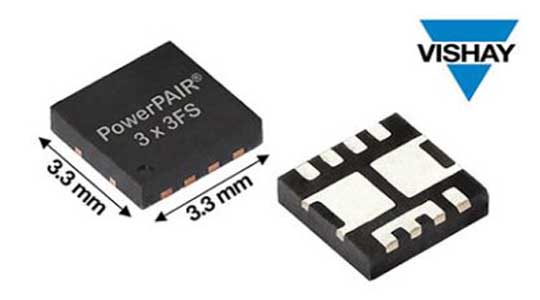
Vishay Intertechnology has introduced two new 30 V symmetric dual n-channel power MOSFETs that combine high and low side TrenchFET® Gen V MOSFETs in a single 3.3 mm by 3.3 mm PowerPAIR® 3x3FS package. For power conversion in computing and telecom applications, the Vishay Siliconix SiZF5300DT and SiZF5302DT increase efficiency while reducing component counts and simplifying designs.
The dual MOSFETs released today can be used in place of two discrete devices in the PowerPAK 1212 package — saving 50 % board space — while offering a 63 % smaller footprint than dual MOSFETs in the PowerPAIR 6x5F. The MOSFETs provide designers with space-saving solutions for synchronous buck converters, point of load (POL) conversion, and DC/DC modules in laptops with USB-C power delivery, servers, DC cooling fans, and telecom equipment. In these applications, the high and low side MOSFETs of the SiZF5302DT form an optimized combination for 50 % duty cycles and best in class efficiency, in particular from 1 A to 4 A, while the SiZF5300DT provides an optimized combination for heavy loads in the 12 A to 15 A range.
The SiZF5300DT and SiZF5302DT leverage Vishay’s 30 V Gen V technology for optimal on-resistance and gate charge. The SiZF5300DT provides typical on-resistance of 2.02 mΩ at 10 V and 2.93 mΩ at 4.5 V, while the SiZF5302DT features on-resistance of 2.7 mΩ at 10 V and 4.4 mΩ at 4.5 V. Typical gate charge for the MOSFETs at 4.5 V is 9.5 nC and 6.7 nC, respectively. The resulting ultra low on-resistance times gate charge — a key figure of merit (FOM) for MOSFETs used in power conversion applications — is 35 % lower than previous-generation solutions with similar on-resistance. For high frequency switching applications, the result is a 2 % increase in efficiency, allowing for efficiency of 98 % at 100 W.
Comparison to Previous-Generation Solution
| Specification / device number | SiZF5302DT(Gen V) | Previous solution(Gen IV) | SiZF5302DT vs previous solution comparison |
| Package | PowerPAIR 3x3FS | PowerPAIR 6x5F | 63 %↓ |
| VDS (V) | 30 | 30 | – |
| RDS(ON) typ.@ 4.5 V (mW) | 4.4 (Channel 1)4.4 (Channel 2) | 4.0 (Channel 1)1.2 (Channel 2) | – |
| Qg @ 4.5 V (nC) | 6.7 (Channel 1)6.7 (Channel 2) | 11 (Channel 1)46 (Channel 2) | – |
| FOM (mΩ*nC) | 29 (Channel 1)29 (Channel 2) | 44 (Channel 1)54 (Channel 2) | 35 % ↓46 % ↓ |
| Efficiency@ 20 VIN / 12.5 VOUT /800 kHZ / 100 W | 98 % | 96 % | 2 %↑ |
The devices’ flip-chip technology enhances thermal dissipation, while their unique pin configuration enables a simplified PCB layout and supports shortened switching loops to minimize parasitic inductance. The SiZF5300DT and SiZF5302DT are 100 % Rg- and UIS-tested, RoHS-compliant, and halogen-free.
Device Specification Table:
| Part number | SiZF5300DT | SiZF5302DT | |
| VDS (V) | 30 | 30 | |
| VGS (V) | + 16 / -12 | + 16 / -12 | |
| RDS(on) typ. (mΩ) @ | 10 V | 2.02 | 2.7 |
| 4.5 V | 2.93 | 4.4 | |
| Qg (Typ.) @ 4.5 V (nC) | 9.5 | 6.7 | |
| ID (A) @ | TA = 25 °C | 125 | 100 |
| TA = 70 °C | 100 | 80 |
Samples and production quantities of the SiZF5300DT and SiZF5302DT are available now. Lead time information may be requested from your Vishay sales contact or by email to pmostechsupport@vishay.com.


