Introduction
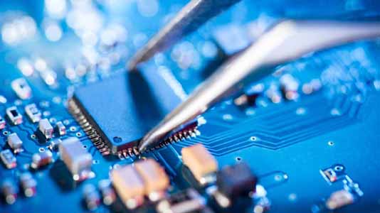
The semiconductor industry is at the heart of technological advancements, and India is emerging as a significant player in this domain. Advanced Integrated Circuit (IC) packaging is a critical aspect of semiconductor manufacturing, enhancing performance, reducing size, and improving power efficiency. This article delves into the latest trends and research in advanced IC packaging, focusing on the Indian market. The Indian semiconductor industry is at a critical juncture, fueled by government initiatives like the Production Linked Incentive (PLI) scheme and an increasing focus on self-reliance. As demand for high-performance computing, artificial intelligence (AI), and 5G technology grows, advanced integrated circuit (IC) packaging is emerging as a key enabler for innovation. This article explores the latest trends in IC packaging in India, backed by recent research and industry developments.
Current Trends in Advanced IC Packaging
2.5D and 3D Packaging: The shift towards 2.5D and 3D packaging is revolutionizing the semiconductor industry. These technologies enable higher performance and power efficiency by stacking multiple chips vertically, reducing the distance between them. The use of Cu-to-Cu hybrid bonding in 3D packaging is particularly noteworthy, offering improved electrical performance and thermal management.

Fan-Out Panel Level Packaging (FOPLP): FOPLP is gaining traction due to its cost-effectiveness and ability to increase area utilization. This technology is particularly beneficial for applications requiring high-density interconnections, such as high-performance computing (HPC) and artificial intelligence (AI) chips.
Material Innovations: The choice of materials plays a crucial role in the success of advanced IC packaging. Silicon, organic, and glass interposers are being explored for 2.5D packaging. Each material has its strengths and challenges, with silicon offering fine routing capabilities, organic interposers providing cost benefits, and glass interposers supporting high dimensional stability.
India’s Semiconductor Packaging Landscape
India is making significant strides in semiconductor manufacturing and packaging. Key initiatives and collaborations are driving this growth:

Vedanta-Foxconn JV: This joint venture focuses on setting up a 28nm technology node semiconductor fab in India, which will bolster the country’s semiconductor manufacturing capabilities.
Tata Electronics: Tata Electronics is exploring advanced semiconductor packaging and system-in-package (SiP) solutions, aiming to position India as a hub for semiconductor innovation.
India Semiconductor Mission (ISM): The ISM is a government-backed initiative to accelerate semiconductor fabrication, design, and advanced packaging capabilities in India. This mission aims to create a robust semiconductor ecosystem, attracting global players and fostering local talent.
Market Outlook and Future Prospects

The global semiconductor market is poised for significant growth, with chip sales expected to reach new heights driven by generative AI and data center build-outs. India’s focus on advanced IC packaging positions it well to capitalize on this growth. The country’s emphasis on developing cutting-edge packaging technologies and fostering collaborations with global leaders will be crucial in achieving this goal.
The Growing Need for Advanced IC Packaging in India
With the rapid expansion of consumer electronics, automotive, and industrial automation sectors, Indian manufacturers and semiconductor design firms are seeking advanced IC packaging solutions. Traditional packaging methods are no longer sufficient to meet the needs of high-performance and miniaturized devices. Advanced packaging technologies such as System-in-Package (SiP), Fan-Out Wafer Level Packaging (FOWLP), and 3D-ICs are transforming the landscape.
Recent Developments and Government Support
Government Initiatives
• The Indian government has approved a $10 billion semiconductor mission to promote domestic chip manufacturing.
• Companies like Tata Electronics and Vedanta-Foxconn are investing heavily in semiconductor packaging and fabrication units.
• The PLI scheme incentivizes firms to establish packaging and assembly facilities in India.
Industry Investments
• TSMC, a global leader in semiconductor packaging, has partnered with several Indian firms to explore advanced packaging solutions.
• India’s growing semiconductor design ecosystem, led by startups and multinational corporations, is pushing for localized packaging solutions to reduce dependency on imports.
Latest Trends in Advanced IC Packaging
3D IC and Heterogeneous Integration
Recent research published in 2024 indicates that 3D IC packaging, which stacks multiple semiconductor dies, improves power efficiency and performance. Leading Indian semiconductor startups are adopting this technology to enhance AI and IoT applications.
Chiplet-Based Design
A 2023 study from SEMI India highlights the growing adoption of chiplet-based architectures, where multiple small chips are integrated into a single package to enhance scalability and reduce production costs.
Examples of successful scaling in IC packaging
Here are some notable examples of successful scaling in IC packaging:
- TSMC’s Advanced Packaging Technologies: Taiwan Semiconductor Manufacturing Company (TSMC) has been a leader in scaling IC packaging. Their Integrated Fan-Out (InFO) technology has been widely adopted for its ability to provide high performance and low power consumption. TSMC’s CoWoS (Chip-on-Wafer-on-Substrate) technology is another example, enabling the integration of multiple chips on a single package, which is crucial for high-performance computing and AI applications.
- Intel’s Foveros Technology: Intel’s Foveros is a 3D packaging technology that allows for the stacking of logic chips on top of each other. This technology enables higher performance and power efficiency by reducing the distance between chips and improving interconnect density. Foveros has been successfully used in Intel’s Lakefield processors.
- Samsung’s Heterogeneous Integration: Samsung has made significant strides in heterogeneous integration, combining different types of chips (e.g., logic, memory) in a single package. Their X-Cube technology, which uses through-silicon vias (TSVs) for vertical interconnects, has been instrumental in achieving high-density integration and improved performance.
- ASE Group’s System-in-Package (SiP): Advanced Semiconductor Engineering (ASE) Group has been a pioneer in System-in-Package (SiP) technology. SiP integrates multiple ICs and passive components into a single package, reducing size and improving performance. ASE’s SiP solutions are widely used in consumer electronics, automotive, and IoT applications.
- These examples highlight how leading companies are leveraging advanced packaging technologies to achieve successful scaling, meeting the demands of modern electronic devices.
Fan-Out Wafer Level Packaging (FOWLP)
FOWLP is gaining traction due to its ability to improve thermal performance and power efficiency. Indian research institutions like IIT Madras and IISc Bangalore are conducting extensive research on developing cost-effective FOWLP solutions.
What are the challenges in IC packaging?
- IC packaging faces several challenges, especially as technology advances and demands for smaller, more efficient devices increase. Here are some of the key challenges:
- Miniaturization and Space Constraints: As consumer devices become more compact, the need for smaller IC packages grows. This miniaturization leads to challenges in maintaining performance and reliability while fitting more components into a smaller space.
- Thermal Management: With increasing power densities, managing heat becomes critical. Effective thermal management is essential to prevent overheating and ensure the longevity and performance of ICs.
- Signal Integrity: High-speed interconnects and the need for faster data transmission can lead to signal integrity issues. Ensuring that signals remain clear and free from interference is a significant challenge.
- Defect Detection: As IC packages become more complex, detecting defects becomes more challenging. Advanced inspection tools, such as infrared, optical, and X-ray technologies, are necessary to identify smaller and more intricate defects.
- Cost and Manufacturing Complexity: Advanced packaging techniques often require sophisticated and expensive equipment. The complexity of manufacturing processes can lead to higher costs and potential yield losses.
- Reliability and Durability: Ensuring the long-term reliability of IC packages is crucial. Factors such as mechanical stress, temperature fluctuations, and environmental conditions can affect the durability of ICs.
- Environmental and Sustainability Concerns: The semiconductor industry faces increasing pressure to adopt environmentally friendly practices. This includes reducing the use of hazardous materials and improving the recyclability of IC packages.
- Addressing these challenges requires continuous innovation and collaboration within the industry to develop new materials, processes, and technologies.
Challenges and Opportunities
Challenges
- High initial capital investment in packaging infrastructure.
- Need for skilled professionals in semiconductor packaging.
- Dependence on imported packaging materials and technology.
Opportunities
- Collaboration between academia and industry to develop indigenous packaging solutions.
- Integration of AI and machine learning in packaging defect detection.
- Expansion of India’s OSAT (Outsourced Semiconductor Assembly and Test) ecosystem.
Conclusion
Advanced IC packaging is transforming the semiconductor industry, and India is at the forefront of this revolution. With ongoing research, innovative technologies, and strategic initiatives, India is well-positioned to become a global leader in semiconductor manufacturing and packaging. As the industry evolves, staying abreast of the latest trends and developments will be key to maintaining a competitive edge. Advanced IC packaging is set to play a pivotal role in India’s semiconductor ambitions. With government backing, increased investments, and a strong R&D push, India is well-positioned to become a major hub for semiconductor packaging. Industry leaders and policymakers must work together to address challenges and accelerate the adoption of cutting-edge packaging technologies.