Atomic force microscopy is a method that enables users to view shapes and textures on surfaces that are too small for the human eye or regular microscopes. AFM works by gently tracing a very small probe across a surface and capturing the changes it detects. These changes are converted into images and measurements, giving a detailed picture of the surface. Despite the advanced science behind it, today’s AFM systems are designed to be as user-friendly as possible and suitable for many research environments.
Did You Know?

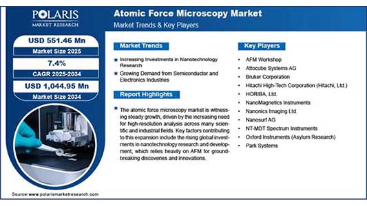
The atomic force microscopy market stood at USD 514.85 million in 2024, according to the latest assessment by Polaris Market Research. The market is anticipated to register a CAGR of 7.4% from 2025 to 2034..
Atomic Force Microscopy Grades
Depending on the level of performance, precision, and features desired, AFM instruments are offered in various grades.
Entry-Level AFM
These systems are designed for basic research, academic use, and routine measurements. They offer clear surface imaging, straightforward controls, and reliable performance for users who need standard analysis without advanced features. Entry-level AFMs are common in university labs and teaching environments.
Mid-Range AFM
Mid-range AFMs feature higher resolution, more measuring modes, and faster operation. They can be used in research centers and industries needing more detailed surface analysis, such as polymer research, material tests, and biological studies. They balance well between affordability and performance; hence, they are very popular among middle-sized laboratories.
High-End AFM
High-end AFMs are used when extremely fine details and high accuracy are needed. They provide superior resolution, advanced modes of imaging, and strong stability, hence finding applications in the development of semiconductors, nanotechnology research, and precision materials science. These systems support highly complex experiments and require trained operators.
Atomic Force Microscopy Applications
AFM is used across many disciplines due to its capability to reveal fine details on different types of surfaces.
Materials Science: AFM is used in the research of metals, ceramics, coatings, polymers, and composites. It gives detailed information about texture, defects, and changes in structure.
Semiconductors and Electronics
AFM supports the development of microchips, sensors, and electronic components by helping engineers inspect surface quality and identify extremely small imperfections.
Life Sciences: AFM enables scientists to investigate cells, tissues, biomolecules, and soft materials without causing damage. It is important for understanding biological surface reactions under various conditions.
Industrial Quality Control: AFM is the technique used by many companies for maintaining product reliability. It supports inspections, testing routines, and surface verification in different manufacturing processes.
Atomic Force Microscopy Market Drivers
Several key factors are encouraging the wider use of AFM systems across industries.
Growing Demand for Miniaturization
The world is developing smaller, thinner, and more complex devices and materials. AFM enables companies to analyze these small structures with precision, thus supporting faster development and better quality control.
View More Information @ https://www.polarismarketresearch.com/industry-analysis/atomic-force-microscopy-market/request-for-sample
Advances in Research and Material Development
With the development of new materials and technologies, especially in nanotechnology, flexible electronics, and biomaterials, researchers require tools of higher accuracy. The AFM offers the resolution necessary to investigate these state-of-the-art surfaces.
Increasing Investments in R&D
Governments, universities, and private companies are increasing their research budgets in various fields, especially semiconductors, healthcare, and advanced materials. As such, AFM instruments appear in most of these investments due to their diverse applications.
Improved Ease of Use
Modern AFM systems are designed with simpler interfaces, more automation, and faster setup; this enhances the learning curve for new users and therefore expands the applicability of the technology.
Atomic Force Microscopy Market Trends
Digital Tools Integration: Advanced software, automated workflows, and data analysis tools are all becoming increasingly available on more AFM systems, improving speed and accuracy.
Portable and Compact AFM Systems: Smaller models of AFM are under development for field use, classroom learning, and low-cost research setups.
Combination with Other Imaging Techniques: AFM is increasingly combined with optical microscopes, electron microscopes, and spectroscopic instruments so that researchers can observe a single sample in several ways.

Conclusion
The Atomic force microscopy market has become essential for understanding surfaces at a level of detail that is necessary in today’s technological and research environment. With its wide range of applications and growing accessibility, AFM will be involved continuously in breakthroughs across materials science, electronics, nanotechnology, and biology. At a time when many industries are working toward smaller, more advanced products, AFM will remain central to innovation, ensuring that analyses are of the highest quality and yielding deeper scientific insight.