As electronics systems become more interconnected, compact and performance-driven, traditional methods of producing flexible circuitry are reaching their limits in cost, speed and environmental impact.While components such as chips and sensors receive much attention, the substrate technologies and patterning processes that enable modern interconnects and circuits are equally central to the future of electronics manufacturing.
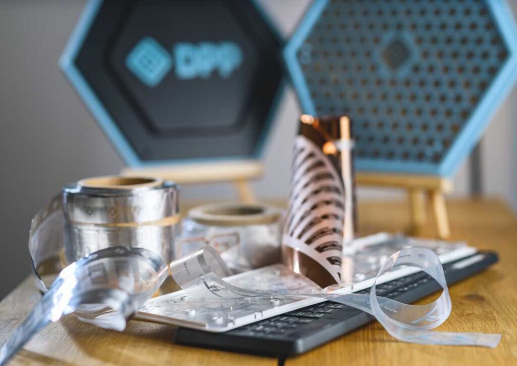
At DP Patterning, we are redefining how conductive traces are formed on flexible substrates through our patented Dry Phase Patterning (DPP) technology. Our approach demonstrates how manufacturing innovation can unlock both commercial and sustainability value across industries from automotive, connectivity to IoT.


Redefining Flexible Substrates and Conductive Patterning
Traditional flex-PCB or flexible printed circuitry often relies on chemical wet etching or printed inks containing noble metals.These processes consume significant energy and water, rely on hazardous chemicals, have long lead times, and depend on volatile material markets.
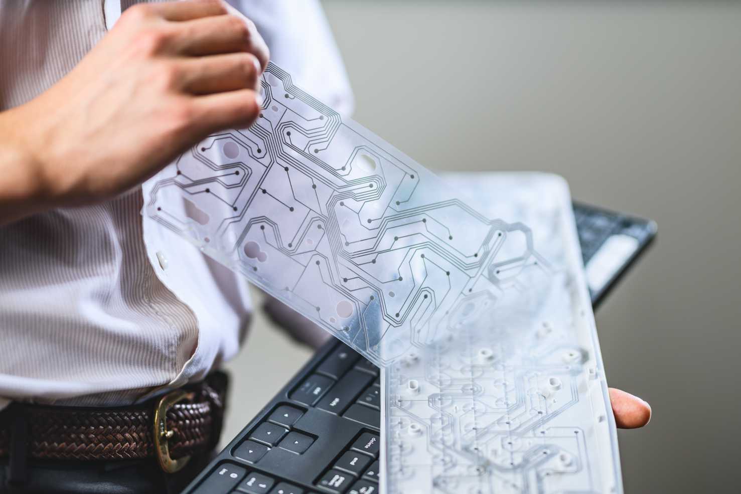
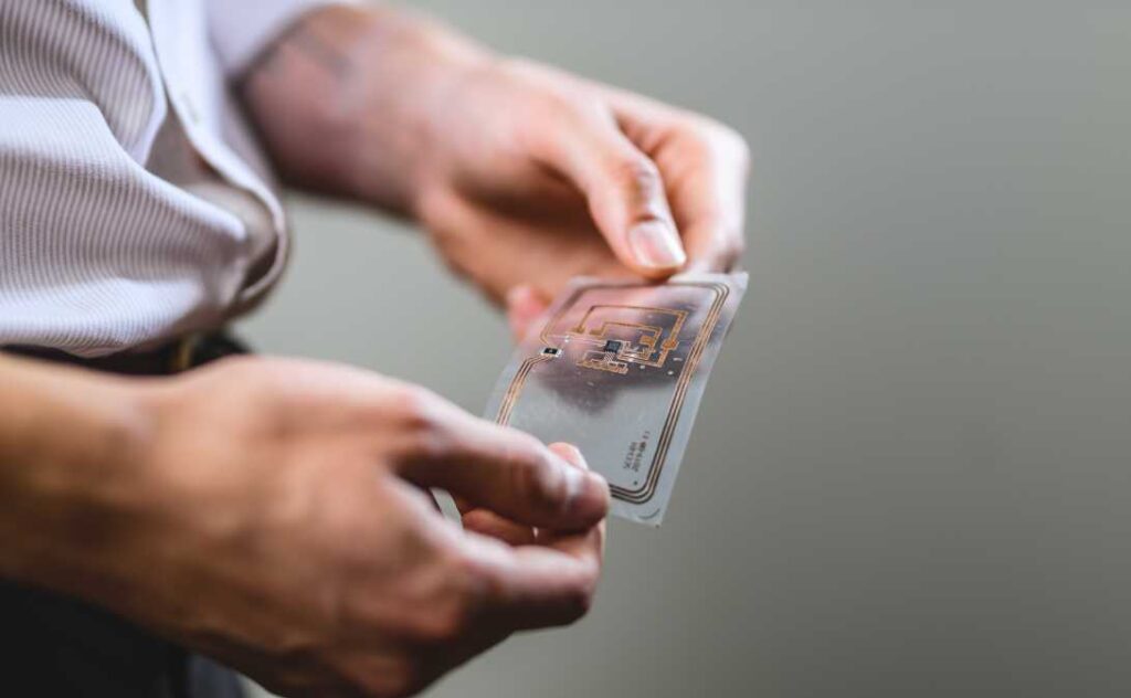
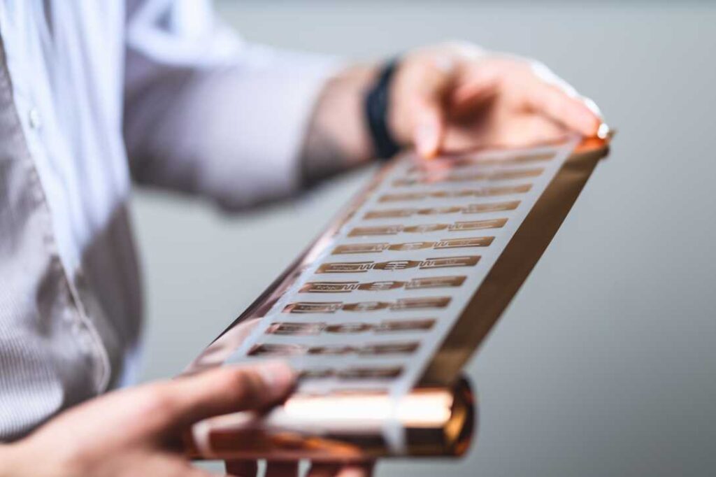
In contrast, Dry Phase Patterning enable a method for precise patterning of conductive traces of aluminium or copper cladded aluminium laminated onto flexible substrates such as PET, PEN, PI etc., without the need for hazardous chemicals or inks.This also allows us to reduce energy consumption and at the same time reduce CO₂ emissions by up to 98% compared to conventional methods, while also cutting production costs.We focus on aluminium and copper cladded aluminium to enable cost savings compared to conventional materials and to address sourcing challenges as well as environmental challenges.The copper cladded aluminium also enables the possibility to solder using a wide range of available solder pastes.
Cost Efficiency Beyond Materials
Cost efficiency today is not only about raw materials. It increasingly depends on:
• Shorter and more resilient supply chains
• High-yield, repeatable processes
• Reduced energy and infrastructure requirements
• Faster time from design to high–volume production
DP Patterning’s method and in-house production of flex electronics offer lightweight, high-performance flexible circuits while allowing us to offer a cost-effective production method. Our approach is particularly relevant for automotive electronics, IoT, connectivity, aerospace, defence, and industrial systems, where balancing weight, margins, volumes, and sustainability is critical.
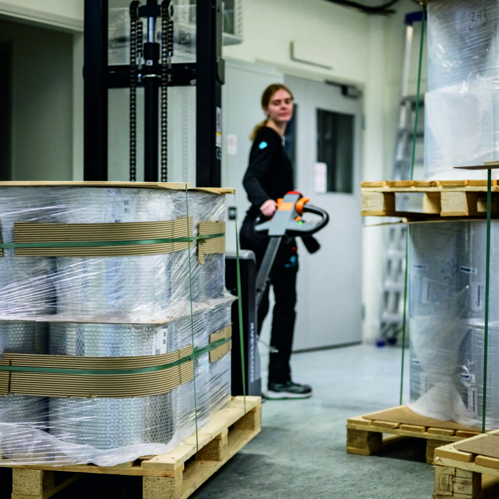
Microplants
A central element of our approach is microplants — compact, localized production units that bring manufacturing closer to end customers.Through these microplants, we achieve shorter, more resilient supply chains, greater flexibility to respond quickly to market and customer needs. By combining DPP with distributed microplant production, we deliver manufacturing that is efficient, sustainable and responsive at scale.

The Path Forward
At DP Patterning, we show that performance, cost and sustainability can all be achieved simultaneously. By rethinking core manufacturing steps and embracing distributed production models, we enable a more resilient, efficient and responsible electronics industry.
As the industry plans for the next decade, the question is no longer if production must change, but how fast.
For more information about DP Patterning visit our webpage (www.dppatterning.com) and follow us on
LinkedIn https://www.linkedin.com/company/dp-patterning/?viewAsMember=true
Talk to a technical expert