Key takeaways:
- Panel-level packaging enables higher area efficiency and scalability for large-format advanced packages
- Transitioning from wafer to panel introduces new challenges in uniformity, yield, and throughput
- Lam’s Salzburg Panel Center of Excellence accelerates panel-level R&D, qualification, and HVM readiness
- Early investment and velocity are critical to avoiding future packaging bottlenecks
Artificial intelligence is rewriting the rules of advanced packaging. Larger dies, denser interconnects, and increasingly complex architectures are moving rapidly from roadmap to reality. As these designs push beyond the physical limits of traditional wafers, panel-level packaging is emerging as a more scalable manufacturing solution for next-generation advanced packages.

For decades, we’ve built the future on a circle. But as advanced packages grow bigger and increasingly complex, round wafers are showing their limitations: edge losses rise, utilization drops, scrap increases, and scaling capacity gets costly and complicated.
One of the biggest shifts ahead may not be about a new material at all. It may be about geometry. As packaging requirements escalate, the industry is being pushed beyond round wafers toward square and rectangular panels as a more scalable manufacturing solution.
“Panel-level packaging is what enables the next generation of large, complex, AI-driven advanced packages to be manufactured efficiently at scale,” says Audrey Charles, SVP of Corporate Strategy and Advanced Packaging. “Leadership at this inflection point comes down to who builds capability—with velocity—before the bottlenecks arrive. That’s why Lam is investing early.”
Why Panel‑Level Packaging Is Critical for Scaling Advanced Packages
Panels are an answer to a scaling problem the industry knows is coming. When advanced packages grow beyond roughly 100 x 100 mm, wafers become inefficient manufacturing vehicles. That’s why panel-level packaging is gaining momentum: it (literally) reshapes the manufacturing canvas so more usable area can be put to work.
But moving from wafer to panel is not a simple format swap. Achieving wafer-level performance at panel scale demands new approaches to process control and yield, all while the semiconductor ecosystem is still deciding standards (e.g., panel size). Moreover, high throughput at panel scale forces a rethink of tool design, automation, and cycle time—while edge control, uniformity, and precision become exponentially harder as substrates get larger.
How Lam’s Salzburg Panel Center Accelerates Panel-Level Packaging Readiness
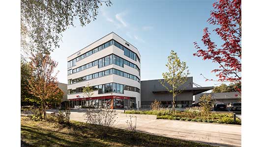
The Panel Center of Excellence in Salzburg, Austria, which Lam officially opened on May 20, is built to shorten that learning curve. The campus brings together manufacturing, clean and grey rooms, storage, and office space—focused mostly on panel R&D, with pilot production lines and engineering testing operations.
The facility also has a state-of-the-art panel-level processing (PLP) laboratory with space dedicated to wet chemical processing. Integrated with Lam’s broader global lab network, the lab is designed to enable rapid learning cycles, customer co‑development, and early qualification.
Accelerating Panel-Level Processing With Lam’s Velocity Model
Velocity—a core theme in Lam’s operating philosophy—means exceeding the pace customers need to hit technology and production milestones. It’s about moving in sync with timelines, reducing friction in development cycles, and making sure the right technical resources are available when inflections arrive.

Panel-level packaging is one of those inflection points. Salzburg is designed to increase velocity in tackling panel-scale challenges by putting the right expertise, tooling, and lab capability in the same place. Faster iteration, earlier qualifications, tighter collaboration, and quicker transfer of what’s learned into the broader portfolio and ecosystem.
What Panel-Level Packaging Means for Advanced Packaging Customers
For customers, the goal is straightforward: make the transition to panels easier, more streamlined. Panel adoption will only accelerate if performance, quality, throughput, and cost can be proven at scale. Salzburg reinforces Lam’s leadership position in panel processing by pairing tool innovation with a dedicated hub for development and collaboration, and by aligning resources ahead of broader industry adoption. It is a concrete example of a multi-year strategy to expand and enhance infrastructure to increase operational and innovation velocity.
The shift from wafer-based to panel-based manufacturing won’t happen overnight. But the direction is clear: By investing early in panels with focused capability and velocity, Lam is helping shape how advanced packaging scales next.
Aaron Fellis is CVP and GM, Global Products