

Artificial intelligence is the biggest demand driver the semiconductor industry has ever seen, accelerating roadmaps in ways that weren’t anticipated five years ago. AI is pushing computational demand at unprecedented scale in hyperscale data centers and is enabling real-time inference at the edge across smartphones, vehicles, and industrial systems. The industry is entering an era in which 3D architectures define the path forward for semiconductors.
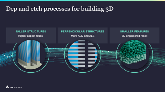
With devices moving to 3D, deposition and etch intensity is expected to rise by roughly a factor of two. As that intensity increases, engineers need to build structures that are taller, more complex, and defined by smaller features. The challenges are reshaping the manufacturing requirements and capabilities needed to scale devices in the 3D era.
What Do We Mean by ‘3D’?
Before turning to the challenges associated with going vertical, it is important to explain what we mean by “3D.” For NAND and DRAM, for example, we’re talking about stacking memory cells, while for logic, we mean 3D transistor architectures.

NAND has been built in 3D for more than a decade, and its evolution continues. Manufacturers are now producing stacks approaching 300 layers, with development already underway toward structures reaching 1,000 layers.
DRAM has been planar for decades, but customers are now shifting from 6F² to 4F² as a key step on the roadmap to fully 3D DRAM architectures. This transition demands high aspect ratio (HAR) etch to form channels, atomic layer deposition (ALD) to fill them, and copper plating to bond CMOS (complementary metal-oxide-semiconductor) wafers to the backside array. As wordlines continue to shrink, rising resistance drives the need for new deposited materials such as molybdenum. As DRAM goes 3D, memory cells will rotate ninety degrees and stack vertically. High bandwidth memory (HBM) is a good example of the shift to 3D already underway today. By stacking multiple DRAM dies vertically and connecting them with dense vertical interconnects, HBM delivers much higher bandwidth in a compact footprint—making it a foundational memory technology for AI systems.
Logic is entering its 3D transition, advancing from FinFET to gate all around (GAA) and, over time, to complementary FET (CFET) architectures. GAA designs rely on specialized atomic layer processes, including layer-by-layer atomic layer etch (ALE) and atomic layer deposition (ALD) to form spacers. These requirements intensify as devices become both taller and smaller in 3D implementations. To relieve routing congestion and improve performance, power delivery can move to the backside of the wafer, further increasing deposition and etch demands.
Advanced packaging, which is experiencing explosive growth, demands heterogeneous integration of stacked chiplets and novel lateral etching and deposition techniques. To bond wafers, new backside deposition steps are needed to flatten the wafer and enable proper alignment. Also, new bevel deposition steps are needed to prevent gaps from occurring when there are differences in thickness at the wafer’s edge.
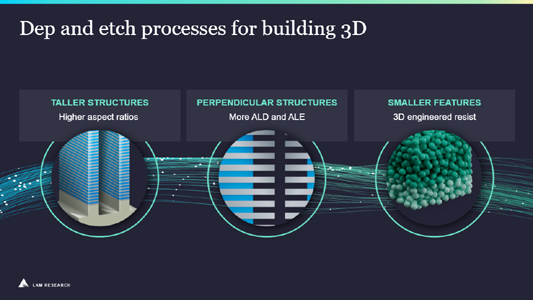
Across the devices there are many challenges in going 3D, among them are these three:
- Building taller structures with increasing aspect ratios
- Enabling perpendicular processing (i.e., laterally)
- Defining ever smaller features
Taller Structures
When you hear 3D, you generally think of the device going taller, and taller means higher aspect ratios. 3D NAND is a perfect example; it requires error-free channel hole etch for extremely vertical channels. Today’s 3D NAND structures have aspect ratios around 50:1. With continued scaling, the industry is moving toward 100:1 in NAND and eventually 200:1 in 3D DRAM, where allowable tilt drops to less than 0.07 degrees.
When we move to 3D DRAM, verticality will be more extreme, which means precision will be mind-blowingly demanding. The geometry is unforgiving: with a 10-micrometer stack, profile tilt must be less than 0.1 degrees. High-volume manufacturing solutions for these aspect ratios do not yet exist. Equipment makers, material suppliers, and device manufacturers must work together to develop them.
The deeper we etch, typically the slower the process goes. In the case of 3D NAND, we’re using cryogenic etching which, seemingly counterintuitively, speeds up the etch process through dielectrics that form the 3D NAND layers. At cryogenic temperatures, a physisorbed layer forms that brings reactants all the way to the bottom of features, improving surface coverage and accelerating etch with minimal distortion. Cryogenic etch can be approximately 2.5 times faster than conventional approaches that can take up to an hour.
Perpendicular Processing With ALD/ALE
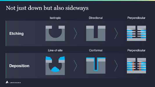
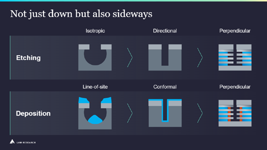
3D architectures require more etching and deposition, requiring going downward in deeper features, and then sideways at 90-degree angles in a process we call perpendicular etch and deposition. In etch, because ions cannot make ninety-degree turns, the techniques that work in 2D are no longer sufficient. Making these turns, which includes repeatability applied uniformly, layer after layer, calls for significantly expanded atomic layer deposition (ALD) and atomic layer etch (ALE) capabilities.
Many of these ALD and ALE technologies are already in production, but further innovation is required without losing precision and quality. This includes new materials being introduced, each requiring novel process development. This creates opportunities for close collaboration between equipment and material suppliers.
Shrinking Features With EUV
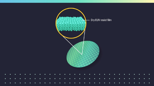
To define the smallest features required for 3D scaling—for example, making a GAA device in logic—extreme ultraviolet (EUV) lithography is essential. As a result, metal oxide resists are moving into production because of their higher EUV sensitivity. Scaling dose and feature size, however, brings new challenges. Low dose, for example, can lead to defects like pinholes, while thinner resist layers leave residues.
To meet the challenges of 3D scaling, we’re also making the resist 3D by grading the material layer by layer, placing more absorber where it is needed to open the process window. This approach requires different precursors and ecosystem support. Lam, who has had a collaborative relationship with ASML going back a decade, has been working with the Dutch company as well as material suppliers to nurture this ecosystem. And last year we signed an agreement with JSR to accelerate deployment of metal oxide resist.
The Path Forward
Deposition and Etch have always been fundamental to semiconductor manufacturing, but today their role in the 3D era is even more critical. These processes are shaping the structures that will power artificial intelligence—translating the promise of AI into silicon reality through close collaboration across the industry.
Vahid Vahedi is Lam Research’s Chief Technology Officer