
In modern cars, sensitive electronic modules are everywhere, yet they remain vulnerable to damage if the vehicle’s battery, typically 12V or 24V, is connected with reversed polarity. This risk is significant because vehicle owners can easily access and incorrectly reinstall batteries, resulting in reverse polarity voltages. To safeguard these expensive electronic modules, input reverse voltage protection (RVP) is an essential design consideration.
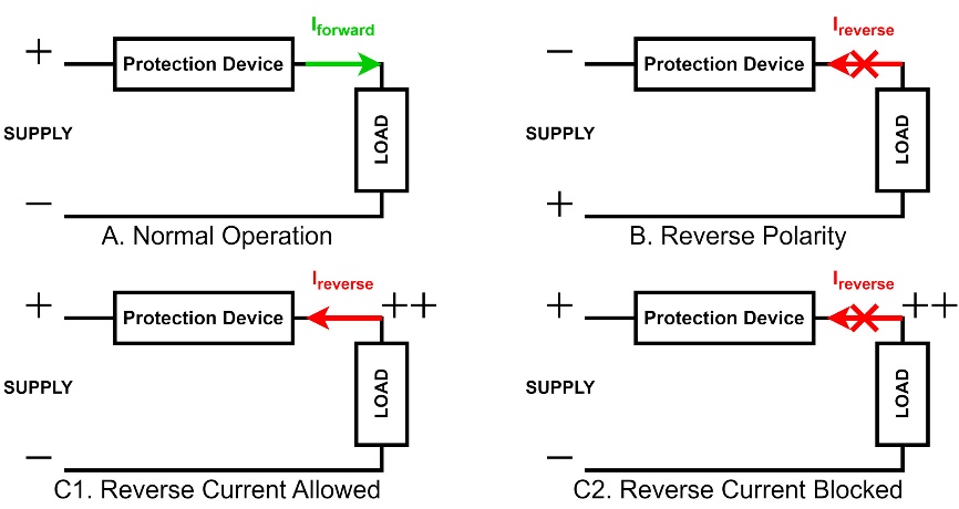
The primary purpose of an RVP device is to allow current flow under normal operating conditions (from positive to negative supply) while blocking current flow if the supply polarity is reversed (Figure 1). Furthermore, RVP solutions must consider scenarios where the load voltage might exceed the supply voltage, for instance, due to back electromotive force (EMF) from a motor, and determine whether to allow or block reverse current flow back to the supply. This article will examine the common approaches to RVP, with a particular emphasis on the nuanced benefits of MOSFET selection for both cost-effectiveness and performance.


Common Approaches to Input Reverse Voltage Protection
As previously mentioned, all RVP protection devices must have the behavior presented in Figure 1, Circuits A and B. The two most common methods for implementing RVP with this behavior involve using either a simple blocking diode or a MOSFET with external control. All approaches to implementing RVP present distinct engineering advantages and disadvantages.
Blocking Diode Approach
The simplest RVP solution involves inserting a single blocking diode in series with the load (Figure 2). This configuration allows current to flow only in forward bias mode, effectively blocking current in reverse bias under all conditions, including the one shown in Figure 1, Circuit C2. This method is the lowest cost solution, especially for low-current applications, and requires the smallest PCB footprint.
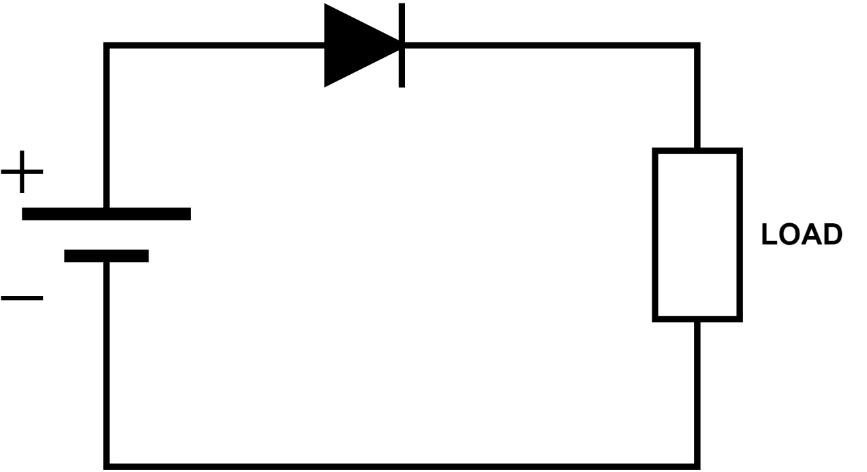
The primary drawback is the power dissipated as heat when the diode is in forward bias, calculated as P = V𝐹 * ILoad. This power loss significantly lowers circuit efficiency and increases the device and board temperature. For instance, powering a 12V, 10A vehicle infotainment system with a Schottky diode (V𝐹=0.46V) results in 4.6W of power loss, leading to 96.16% efficiency. An SBRT, from Diodes Incorporated, while better (V𝐹=0.37V, 3.7W loss, 96.92% efficiency), still dissipates considerable power.
Schottky diodes, despite their low V𝐹, can exhibit high reverse current leakage at elevated temperatures, making them susceptible to thermal runaway. Moreover, high-current applications necessitate larger diodes and increased heatsinking copper area, which can offset the initial footprint advantage.
MOSFET-Based Approaches
MOSFETs offer a more efficient alternative for RVP, significantly reducing power dissipation compared to diodes. When used as an ideal diode in series with a load, a MOSFET’s power loss is determined by its intrinsic ON resistance (RDS(ON)) and the load current (𝑃𝑙𝑜𝑠𝑠 = 𝐼𝐿𝑜𝑎𝑑² * 𝑅𝐷𝑆(𝑂𝑁)). This lower power dissipation translates to a reduced temperature increase and potentially less heatsinking requirements.
Two common MOSFET-based RVP circuits are:
1. Self-Biased P-Channel MOSFET Circuit: This simple high-side configuration uses a P-channel MOSFET, often with a Zener diode for gate protection (Figure 3). Under normal operation (Figure 1, Circuit A), the P-channel MOSFET turns ON, allowing forward current flow with losses determined by RDS(ON).
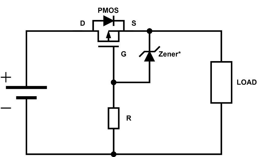
In reverse polarity, the MOSFET remains OFF, and its body diode blocks current. This circuit allows reverse current to flow back to the supply (Figure 1, Circuit C1) if the load voltage exceeds the supply voltage, which may not be desired depending on the application. The main advantages of this approach are lower power dissipation compared to a diode, simpler circuit design, and straightforward sizing for different load currents. However, it is more expensive than a simple diode.
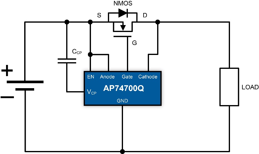
2. Ideal Diode Controller with N-Channel MOSFET Circuit: Ideal diode controllers, such as Diodes Incorporated’s AP74700AQ, actively manage an external N-channel MOSFET to provide high-side RVP (Figure 4). The ideal diode uses an internal charge pump to drive the N-channel MOSFET gate.

During normal operation, it can regulate the voltage differential across the MOSFET to 20mV at low load currents or drive the MOSFET fully ON, where the voltage drop is limited by its RDS(ON) at higher currents. Crucially, if a reverse voltage is detected (greater than 10mV), the controller turns the MOSFET OFF, blocking reverse currents under both reverse polarity conditions and when the load voltage exceeds the supply voltage (Figure 1, Circuits B and C2).
For high current (high power) applications, this solution offers the lowest power dissipation among the discussed methods, regulates MOSFET enhancement, provides fast MOSFET turn-off, and blocks reverse currents (Figure 1, Circuit C2). However, suppose the N-channel MOSFET is in the 20mV regulated region. In that case, it may have a higher power dissipation than a P-channel MOSFET that is fully turned on and has a voltage drop of, for example, 10mV across itself.
N-channel MOSFETs are generally smaller and cheaper than P-channel MOSFETs with comparable RDS(ON), contributing to lower design costs. For the 12V, 10A infotainment system example, a P-channel MOSFET, such as the DMP4013LFGQ from Diodes Incorporated, dissipates only 1.3W (98.92% efficiency). In contrast, an N-channel MOSFET, the DMTH43M8LFGQ, also from Diodes, dissipates just 0.3W (99.75% efficiency), making it the most efficient solution.
At high currents, the ideal diode controller solution will be cheaper than a diode suitable for those currents, but more expensive than a diode at low currents. It also blocks reverse currents (C1), which might not be desirable for applications requiring current flow back to the supply. The total solution footprint can also be larger than a single diode due to the controller and external components.
MOSFET Selection for Cost-Effectiveness and Performance
Selecting the appropriate MOSFET is key for optimizing both the cost and performance of an RVP solution, particularly when using an ideal diode controller (Figure 5).
Voltage Rating
The MOSFET’s drain-source voltage (VDS) rating is a critical initial parameter. It must not only withstand the normal battery voltage but also account for potential voltage doubling in reverse polarity scenarios (e.g., a fully charged load capacitance at +12V with a -12V input results in a 24V differential across the MOSFET). Furthermore, automotive systems must comply with standards like ISO7637-2 and ISO16750-2, which specify various pulses and spikes, necessitating a higher voltage rating.
As a general recommendation for automotive applications, a 40V MOSFET is typically chosen for a 12V nominal rail, 60V for 24V, and 80V or 100V for 48V systems. The AP74700AQ ideal diode controller, rated at 65V (max.), can withstand a -65V rail voltage, suggesting that a 60V MOSFET may be chosen even for a 12V nominal rail for added robustness.
Current Handling and RDS(ON): The Cost-Performance Trade-Off
The next crucial parameter is the MOSFET’s RDS(ON), which directly relates to its ability to support the load current and its power dissipation.
Understanding Operating Modes: The AP74700AQ ideal diode controller operates the N-channel MOSFET in two modes:
- Regulated Mode: At low load currents, the controller actively maintains the voltage drop across the MOSFET at a minimal 20mV.
- RDS(ON) Limited Mode: At higher currents, the voltage drop across the MOSFET is dictated by its inherent RDS(ON), effectively acting as a resistor (V = ILoad * RDS(ON)). Power loss in this mode is calculated as 𝐼𝐿𝑜𝑎𝑑² * 𝑅𝐷𝑆(𝑂𝑁).
Cost-Effectiveness at Low Currents: A key insight for cost-effective design is that a lower RDS(ON) typically translates to a larger die size, a larger package, and consequently, a higher cost. In low-current conditions, where the ideal diode controller is actively regulating the voltage drop to 20mV, there is no significant performance advantage in using a very low RDS(ON) device.
The voltage drop is primarily controlled by the AP74700AQ, not the MOSFET’s inherent resistance. Therefore, selecting an unnecessarily low RDS(ON) MOSFET in this region would incur extra cost without providing a proportional performance benefit.
This allows designers to optimize for cost by choosing a MOSFET that adequately meets requirements without over-specifying. For example, if a 15mΩ device is mostly regulated at 20mV and only exceeds this slightly during current peaks, a 10mΩ device, while offering a marginal further improvement, might not be cost-effective for that current level.
Performance and Efficiency at High Currents: Conversely, in high-current applications (e.g., 20A, 30A, 40A, or more for systems like modern car infotainment systems or EVs), the MOSFET will frequently operate in the RDS(ON) limited mode. In these scenarios, the lowest possible RDS(ON) is critical.
The I²R power loss becomes substantial, and a lower RDS(ON) directly reduces this power loss, resulting in significantly improved efficiency and lower thermal stress. This minimization of losses is crucial for maximizing range in EVs and enhancing overall performance in high-power automotive applications.
Lower power dissipation also translates to a much lower temperature increase for the MOSFET, potentially reducing the need for extensive heatsinking copper area or allowing for smaller package sizes. While these MOSFETs may have a higher component cost, the indirect savings in thermal management, PCB space, and improved system reliability can make them the most cost-effective solution overall for high-power demands.
The decision regarding the ideal RDS(ON) involves a careful trade-off between maximizing efficiency and managing cost. A 25mΩ MOSFET, for example, represents a significant efficiency improvement over a traditional diode. Designers must weigh whether the incremental efficiency gains offered by an even lower RDS(ON) device justify the additional cost, based on the specific current profile and design objectives of the application.
Packaging and Thermal Considerations
Beyond electrical characteristics, the MOSFET’s package type and the amount of copper area on the PCB significantly influence its thermal performance. Power dissipation calculations (VI for regulated mode or I²R for RDS(ON)– limited mode) are essential for determining the required thermal impedance (RθJA) and selecting the most appropriate package. Diodes Incorporated’s PowerDI®3333 and PowerDI®5060 packages are noted for their efficient PCB layout alignment with ideal diode controllers like the AP74700AQ. It is also crucial to account for the thermal coefficient of RDS(ON), which typically increases with temperature, during calculations.
Conclusion
Input reverse voltage protection is indispensable for safeguarding sensitive automotive electronics against incorrect battery connections. While simple diodes offer a low-cost, low-footprint solution for low current applications, their significant power dissipation at higher currents makes them inefficient. MOSFET-based solutions, particularly those employing ideal diode controllers with N-channel MOSFETs, provide substantially lower power dissipation and higher efficiency, making them ideal for high-power automotive systems and EVs.
The selection of the MOSFET’s RDS(ON) is a critical design choice that directly impacts both performance and cost-effectiveness. For low-current applications where the ideal diode controller actively regulates the voltage drop, designers can achieve cost savings by avoiding unnecessarily low RDS(ON) devices without compromising performance.
Conversely, for high-current applications, prioritizing the lowest possible RDS(ON) is paramount for maximizing efficiency, minimizing power loss, and managing thermals. All these ultimately contribute to overall system performance and can lead to indirect cost benefits from reduced thermal management requirements.
The optimal RVP solution for any given application is a multifaceted decision. It is a fine balance of factors such as cost, solution size, efficiency, power dissipation requirements, circuit complexity, and desired features.