Electronics Era

  • About Us
  • Advertise with Us
  • Contact Us
  • e-Mag
  • Webinars
Header logo on website
Advertisement
Advertisement
Menu
  • Home
  • News
    • Industry News
    • Product News
  • TECH ROOM
    • Sensor
    • VR / AR
    • Embedded
    • Medical Electronics
    • Industry 4.0
    • Robotic
    • Automation
    • Smart Machine
    • Component
    • MCU
    • Manufacturing
    • Aerospace & Defence
    • Security
    • Policy
    • RENEWABLES
      • Sustainability
  • Semiconductor
    • AUTOMOTIVE ELECTRONICS
      • EVs
      • HEVs
      • ADAS
      • Connected Cars
    • IoT-Internet of Things
      • Development Kit
      • IoT Design
    • Power Electronics
      • AC-DC/DC-DC Converters
      • Mosfets
      • IGBTs
      • LEDs
  • T & M
    • 5G testing
    • Oscilloscopes
    • SDN & NFV
    • RF & Wireless
  • AI/ML
  • Telecom
    • 5G/6G
  • Future Tech
    • Data Center
    • Cloud Computing
    • Big Data Analytics
  • Webinars
  • Editor’s Pick
    • Tech Article
    • Tech Blog
    • White Papers
    • EE-Tech Talk
    • Market Research
    • Videos
  • EE Awards
    • EE Awards 2025
    • EE Awards 2024
  • MORE
    • E-Mag
    • Events
    • MAGAZINE Subscription
    • Contact Us
Home T & M

Keysight Unveils 3D Interconnect Designer for Chiplet and 3DIC Advanced Package Designs

Solution addresses design bottleneck by automating complex workflows

Nimish by Nimish
February 19, 2026
in T & M
Reading Time: 2 mins read
Keysight Technologies

Keysight 3D Interconnect Designer for Chiplet and 3DIC Advanced Package Designs

Share on FacebookShare on TwitterShare on LinkedIn

India – Keysight Technologies, Inc.  today introduced 3D Interconnect Designer, a new addition to its Electronic Design Automation (EDA) portfolio. The solution addresses the mounting complexity of designing 3D interconnects for high-chiplet and 3DIC advanced packages used in AI infrastructure and data center applications.

As chiplet architectures are increasingly adopted, engineers face complex 3D interconnect designs for multi-die and stacked-die applications which traditional workflows struggle to handle efficiently. As a result, teams spend significant time manually optimizing the interconnects that include vias, transmission lines, solder balls, and micro-bumps while ensuring signal and power integrity in densely packed systems. This results in more design spins and longer product development cycles, creating a bottleneck that can delay product launches and increase development costs.

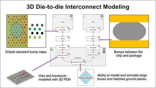
Keysight EDA software streamlines the process with a dedicated workflow for designing and optimizing 3D interconnects accurately. The tool handles complex geometries, including hatched or waffled ground planes, which are critical to overcome manufacturing and fabrication constraints, especially silicon processes such as interposers and bridges, in advanced package designs. By enabling engineers to quickly design, optimize, and validate 3D interconnects used in chiplets and 3DICs, it minimizes iterations and speeds time-to-market.

Key benefits include:

  • Accelerates Design Cycles: Streamlined automation removes time‑consuming manual steps in 3D interconnect design, minimizing errors and boosting first‑pass success
  • Reduced Compliance Risk: Validates designs against emerging standards such as UCIe and BoW, ex VTF (Voltage Transfer Function), early in the lifecycle, reducing the risk of late-stage failures that lead to costly redesigns
  • Predicts Performance Accurately: Electromagnetic-based simulation provides precise electrical analysis of printed circuit boards (PCB) and package 3D interconnect designs

The solution integrates with Keysight’s EDA tools as well as supporting the standalone version, enabling teams to incorporate 3D interconnect design and optimization into existing workflows. When combined with Chiplet PHY Designer, engineers can design and optimize 3D interconnects specifically for chiplets and three-dimensional integrated circuits (3DICs), ensuring accuracy and reducing costly iterations in multi-die systems.

Nilesh Kamdar, EDA Design and Verification General Manager at Keysight, said:

“With today’s complexity, manual 3D interconnect design and optimization have become a significant bottleneck. By streamlining the process and providing early insights into potential issues like signal and power integrity, we’re enabling engineers to get products to market faster and deliver compliant designs on tighter timelines.”

Tags: chipletElectronic Design Automation (EDA)Keysight Technologies
Nimish

Nimish


Join Our Newsletter

* indicates required
Electronics Era

Electronics Era, India's no.1 growing B2B news forum on Electronics and Cutting Edge Technology is exploring the editorial opportunity for organizations working in the Electronics Manufacturing Services(EMS) Industry.

Follow Us

Browse by Category

  • 5G testing
  • 5G/6G
  • AC-DC/DC-DC Converters
  • ADAS
  • Aerospace & Defence
  • AI/ML
  • Automation
  • AUTOMOTIVE ELECTRONICS
  • Big Data Analytics
  • Blockchain
  • Cloud Computing
  • Component
  • Connected Cars
  • Data Center
  • Editor's Desk
  • EE-Tech Talk
  • Electronics Components
  • Embedded
  • EVs
  • Future Tech
  • HEVs
  • Industry 4.0
  • Industry News
  • IoT Design
  • IoT-Internet of Things
  • LED & Lighting
  • LEDs
  • Manufacturing
  • Market Research
  • MCU
  • Medical Electronics
  • Mosfets
  • News
  • Oscilloscopes
  • Policy
  • Power Electronics
  • Product News
  • RENEWABLES
  • RF & Wireless
  • Robotic
  • SDN & NFV
  • Security
  • Semiconductor
  • Sensor
  • Smart Machine
  • SMT/PCB/EMS
  • Sustainability
  • T & M
  • Tech Article
  • Tech Blog
  • TECH ROOM
  • Telecom
  • Uncategorized
  • VR / AR
  • White Papers

Recent News

Tata Elxsi

Tata Elxsi and Sky Mark a Major Milestone in AI-led Autonomous Network Transformation with NEURON

June 24, 2026
CloudBuddi

AppSquadz Brings AI-Powered FinOps to the Mainstream with CloudBuddi

June 24, 2026
  • About Us
  • Advertise with Us
  • Contact Us

© 2022-23 TechZone Print Media | All Rights Reserved

No Result
View All Result
  • Home
  • News
    • Industry News
    • Product News
  • TECH ROOM
    • Sensor
    • VR / AR
    • Embedded
    • Medical Electronics
    • Industry 4.0
    • Robotic
    • Automation
    • Smart Machine
    • Component
    • MCU
    • Manufacturing
    • Aerospace & Defence
    • Security
    • Policy
    • RENEWABLES
      • Sustainability
  • Semiconductor
    • AUTOMOTIVE ELECTRONICS
      • EVs
      • HEVs
      • ADAS
      • Connected Cars
    • IoT-Internet of Things
      • Development Kit
      • IoT Design
    • Power Electronics
      • AC-DC/DC-DC Converters
      • Mosfets
      • IGBTs
      • LEDs
  • T & M
    • 5G testing
    • Oscilloscopes
    • SDN & NFV
    • RF & Wireless
  • AI/ML
  • Telecom
    • 5G/6G
  • Future Tech
    • Data Center
    • Cloud Computing
    • Big Data Analytics
  • Webinars
  • Editor’s Pick
    • Tech Article
    • Tech Blog
    • White Papers
    • EE-Tech Talk
    • Market Research
    • Videos
  • EE Awards
    • EE Awards 2025
    • EE Awards 2024
  • MORE
    • E-Mag
    • Events
    • MAGAZINE Subscription
    • Contact Us

© 2022-23 TechZone Print Media | All Rights Reserved

Advertisement
Advertisement