Electronics Era

  • About Us
  • Advertise with Us
  • Contact Us
  • e-Mag
  • Webinars
Header logo on website
Advertisement
Advertisement
Menu
  • Home
  • News
    • Industry News
    • Product News
  • TECH ROOM
    • Sensor
    • VR / AR
    • Embedded
    • Medical Electronics
    • Industry 4.0
    • Robotic
    • Automation
    • Smart Machine
    • Component
    • MCU
    • Manufacturing
    • Aerospace & Defence
    • Security
    • Policy
    • RENEWABLES
      • Sustainability
  • Semiconductor
    • AUTOMOTIVE ELECTRONICS
      • EVs
      • HEVs
      • ADAS
      • Connected Cars
    • IoT-Internet of Things
      • Development Kit
      • IoT Design
    • Power Electronics
      • AC-DC/DC-DC Converters
      • Mosfets
      • IGBTs
      • LEDs
  • T & M
    • 5G testing
    • Oscilloscopes
    • SDN & NFV
    • RF & Wireless
  • AI/ML
  • Telecom
    • 5G/6G
  • Future Tech
    • Data Center
    • Cloud Computing
    • Big Data Analytics
  • Webinars
  • Editor’s Pick
    • Tech Article
    • Tech Blog
    • White Papers
    • EE-Tech Talk
    • Market Research
    • Videos
  • EE Awards
    • EE Awards 2025
    • EE Awards 2024
  • MORE
    • E-Mag
    • Events
    • MAGAZINE Subscription
    • Contact Us
Home Semiconductor

SecureFoundry Redefines Chipmaking with Hyper-Beam Array Lithography System

First HBA lithography system in the U.S. harnesses 65,000 parallel beams for unmatched flexibility, rapid prototyping and die-level traceability

Vishaka Vardhan by Vishaka Vardhan
October 7, 2025
in Semiconductor
Reading Time: 3 mins read
hba tool
Share on FacebookShare on TwitterShare on LinkedIn

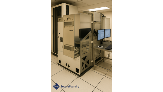
FORT WORTH, Texas — SecureFoundry has introduced its Hyper-Beam Array (HBA) lithography system, based on a proven architecture originally pioneered in Europe. HBA is a new class of lithography, distinct from both single-beam and multibeam approaches, operating with tens of thousands of independently controlled beams and delivering capabilities at a scale no electron-beam technology can match.

“During the system’s characterization, we demonstrated the ability to fully pattern a 100mm wafer in just 15 minutes,” said Lex Keen, founder and CEO of SecureFoundry. “The HBA tool enables wafer-scale integration, advanced fan-out packaging, and multiple design variations in a single run—delivering unmatched flexibility and faster innovation. The HBA tool allows AI chip designers to experiment with slight design variations across a single wafer, enabling exploration of ‘AI personalities’ and rapid feedback on performance outcomes. Unlike multibeam systems with only a handful of beams, HBA lithography represents a different class altogether, built for both advanced and legacy nodes, throughput and reliability.”

Unlike traditional photolithography, which requires costly masks and has long lead times, HBA lithography uses 65,000 parallel electron beams to pattern wafers directly. Each beam is independently controlled. The system scans the wafer in two passes, automatically compensating for any missed pattern, ensuring reliability and consistency across the system as well as enabling fine-grained control and high-fidelity pattern placement. This architecture is specifically optimized for mixed-volume manufacturing and security-critical use cases where flexibility, traceability and repeatability are paramount.

The SecureFoundry HBA lithography system supports research institutions, defense contractors and commercial partners seeking agile, onshore solutions. The tool fills a gap in the semiconductor supply chain between design, research and development, and commercial production, enabling highly custom chip designs. It is optimized for nodes between 22nm and 65nm, can print on 100mm to 300mm substrates, and can pattern silicon or compound silicon substrates. Its software-defined patterning architecture enables design flexibility, while built-in die-level traceability and digital provenance address growing requirements around trusted supply chains and device authentication.

“For defense and security applications, every die must be accounted for,” said Keen. “This system gives us a fully auditable chain of custody from design to wafer.”

The HBA lithography system integrates seamlessly with existing industry-standard EDA workflows while also offering design optimization for customers requiring accelerated iteration or advanced security constraints. The system also allows for hybrid processing capabilities. Some layers of a device may benefit from traditional mask-based lithography methods, while others gain speed and cost advantages through HBA lithography. SecureFoundry’s platform adapts to fit the customer’s node, production volume and budget, unlocking further flexibility for engineers.

“Our approach will create new customers for large, leading-edge fabs,” said Keen. “The HBA lithography system provides access to manufacturing capabilities that are needed to commercialize new chip technologies, allowing companies to build demand and ultimately transition manufacturing toward high-volume fabs. An increase in new technologies demanding high-volume services, enabled by our technology, is a collaborative win for the industry. By removing barriers to entry for both emerging and legacy devices, we fill a critical void in the ecosystem.”

The HBA lithography system is operated exclusively within U.S.-based, secure facilities, ensuring compliance with all defense and export control regulations.

For more information about HBA lithography, contact [email protected].

Tags: Lithography SystemSecureFoundrySemiconductor Technology
Vishaka Vardhan

Vishaka Vardhan

[adrotate banner="216"]

Join Our Newsletter

* indicates required
Electronics Era

Electronics Era, India's no.1 growing B2B news forum on Electronics and Cutting Edge Technology is exploring the editorial opportunity for organizations working in the Electronics Manufacturing Services(EMS) Industry.

Follow Us

Browse by Category

  • 5G testing
  • 5G/6G
  • AC-DC/DC-DC Converters
  • ADAS
  • Aerospace & Defence
  • AI/ML
  • Automation
  • AUTOMOTIVE ELECTRONICS
  • Big Data Analytics
  • Blockchain
  • Cloud Computing
  • Component
  • Connected Cars
  • Data Center
  • Editor's Desk
  • EE-Tech Talk
  • Electronics Components
  • Embedded
  • EVs
  • Future Tech
  • HEVs
  • Industry 4.0
  • Industry News
  • IoT Design
  • IoT-Internet of Things
  • LED & Lighting
  • LEDs
  • Manufacturing
  • Market Research
  • MCU
  • Medical Electronics
  • Mosfets
  • News
  • Oscilloscopes
  • Policy
  • Power Electronics
  • Product News
  • RENEWABLES
  • RF & Wireless
  • Robotic
  • SDN & NFV
  • Security
  • Semiconductor
  • Sensor
  • Smart Machine
  • SMT/PCB/EMS
  • Sustainability
  • T & M
  • Tech Article
  • Tech Blog
  • TECH ROOM
  • Telecom
  • Uncategorized
  • VR / AR
  • White Papers

Recent News

Ingram Micro

Achievers World Honors Ingram Micro’s Sanjib Sahoo as Business Excellence Icon of the World

June 3, 2026
NeoCortec

NeoMesh from NeoCortec powers e-IoT platform from Endrich Bauelemente

June 3, 2026
  • About Us
  • Advertise with Us
  • Contact Us

© 2022-23 TechZone Print Media | All Rights Reserved

No Result
View All Result
  • Home
  • News
    • Industry News
    • Product News
  • TECH ROOM
    • Sensor
    • VR / AR
    • Embedded
    • Medical Electronics
    • Industry 4.0
    • Robotic
    • Automation
    • Smart Machine
    • Component
    • MCU
    • Manufacturing
    • Aerospace & Defence
    • Security
    • Policy
    • RENEWABLES
      • Sustainability
  • Semiconductor
    • AUTOMOTIVE ELECTRONICS
      • EVs
      • HEVs
      • ADAS
      • Connected Cars
    • IoT-Internet of Things
      • Development Kit
      • IoT Design
    • Power Electronics
      • AC-DC/DC-DC Converters
      • Mosfets
      • IGBTs
      • LEDs
  • T & M
    • 5G testing
    • Oscilloscopes
    • SDN & NFV
    • RF & Wireless
  • AI/ML
  • Telecom
    • 5G/6G
  • Future Tech
    • Data Center
    • Cloud Computing
    • Big Data Analytics
  • Webinars
  • Editor’s Pick
    • Tech Article
    • Tech Blog
    • White Papers
    • EE-Tech Talk
    • Market Research
    • Videos
  • EE Awards
    • EE Awards 2025
    • EE Awards 2024
  • MORE
    • E-Mag
    • Events
    • MAGAZINE Subscription
    • Contact Us

© 2022-23 TechZone Print Media | All Rights Reserved

Advertisement
Advertisement