Electronics Era

  • About Us
  • Advertise with Us
  • Contact Us
  • e-Mag
  • Webinars
Header logo on website
Advertisement
Advertisement
Menu
  • Home
  • News
    • Industry News
    • Product News
  • TECH ROOM
    • Sensor
    • VR / AR
    • Embedded
    • Medical Electronics
    • Industry 4.0
    • Robotic
    • Automation
    • Smart Machine
    • Component
    • MCU
    • Manufacturing
    • Aerospace & Defence
    • Security
    • Policy
    • RENEWABLES
      • Sustainability
  • Semiconductor
    • AUTOMOTIVE ELECTRONICS
      • EVs
      • HEVs
      • ADAS
      • Connected Cars
    • IoT-Internet of Things
      • Development Kit
      • IoT Design
    • Power Electronics
      • AC-DC/DC-DC Converters
      • Mosfets
      • IGBTs
      • LEDs
  • T & M
    • 5G testing
    • Oscilloscopes
    • SDN & NFV
    • RF & Wireless
  • AI/ML
  • Telecom
    • 5G/6G
  • Future Tech
    • Data Center
    • Cloud Computing
    • Big Data Analytics
  • Webinars
  • Editor’s Pick
    • Tech Article
    • Tech Blog
    • White Papers
    • EE-Tech Talk
    • Market Research
    • Videos
  • EE Awards
    • EE Awards 2025
    • EE Awards 2024
  • MORE
    • E-Mag
    • Events
    • MAGAZINE Subscription
    • Contact Us
Home Telecom 5G/6G

Selected for NEDO’s Research and Development Project of the Enhanced Infrastructures for Post-5G Information and Communication Systems

Vishaka Vardhan by Vishaka Vardhan
December 3, 2025
in 5G/6G
Reading Time: 3 mins read
NEDO
Share on FacebookShare on TwitterShare on LinkedIn

NGK INSULATORS, LTD. has announced that its Research and Development of Thin Film Lithium Niobate (TFLN) Optical Technology for the Industrialization of Optical Quantum Computers has been selected for the Research and Development Project of the Enhanced Infrastructures for Post-5G Information and Communication Systems (Quantum Industrialization) of the New Energy and Industrial Technology Development Organization (NEDO). Harnessing the bonded wafer technology it has developed over many years, NGK will work on the development of photonic integrated circuits. Through this project, NGK will accelerate the practical application of optical quantum computers and contribute to building the information processing infrastructure that will support next-generation AI.

Advances in generative AI have increased electricity consumption at data centers around the world, and the resulting environmental burden and higher energy costs have emerged as social issues. The high-speed computing capabilities of quantum computers are attracting attention as a potential solution to these issues.

Conventional quantum computers operate at extremely low temperatures, requiring massive cooling equipment and tremendous energy costs. In contrast, optical quantum computers can operate at room temperature, eliminating the need for cooling equipment and enabling a substantial reduction in installation space and greater energy efficiency. Moreover, because they are highly compatible with existing optical fiber, optical quantum computers are regarded as a promising next-generation technology for implementation in society.

The project will work to develop photonic integrated circuits with the aim of achieving practical application of optical quantum computers, which have so far remained at the proof-of-principle stage. In addition, by promoting global standardization led by domestic manufacturers, the project seeks to establish a robust supply chain.

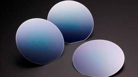
In the project, NGK will be responsible for developing TFLN* wafers, which are essential to integrated circuits used in optical quantum computers. Leveraging the direct bonding technology cultivated through the development of bonded wafers for surface acoustic wave (SAW) filters, NGK can bond different materials with high precision at room temperature without using adhesives, thereby ensuring the material properties of TFLN and achieving high reliability. Furthermore, by applying its ultra-precision-polishing technology, which enables the functional layer to be fabricated as a uniform thin film at the nanometer level, NGK will contribute to the thinning of wafers. Based on these technologies, NGK will develop eight-inch TFLN wafers, which will pave the way for reducing mass production costs and enhancing competitiveness.

The project will be implemented under a 3-year plan covering FY2025 to FY2027, with NGK working in collaboration with multiple companies and research organizations. Guided by the NGK Group Vision: Road to 2050, the NGK Group aims to achieve a business structure conversion toward the carbon neutrality (CN) and digital society (DS) domains. Through this project, NGK will accelerate the creation of new products and new businesses based on themes that support the NGK Group’s growth and contribute to the realization of a sustainable society.

■ Project Structure

  • NGK INSULATORS, LTD. (project lead)
  • YAMAJU CERAMICS CO., LTD.
  • OXIDE Corporation
  • Hamamatsu Photonics K.K.
  • National Institute of Advanced Industrial Science and Technology (AIST) (joint research partner)
Tags: 5GNEDOTFLNThin Film Lithium Niobate
Vishaka Vardhan

Vishaka Vardhan


Join Our Newsletter

* indicates required
Electronics Era

Electronics Era, India's no.1 growing B2B news forum on Electronics and Cutting Edge Technology is exploring the editorial opportunity for organizations working in the Electronics Manufacturing Services(EMS) Industry.

Follow Us

Browse by Category

  • 5G testing
  • 5G/6G
  • AC-DC/DC-DC Converters
  • ADAS
  • Aerospace & Defence
  • AI/ML
  • Automation
  • AUTOMOTIVE ELECTRONICS
  • Big Data Analytics
  • Blockchain
  • Cloud Computing
  • Component
  • Connected Cars
  • Data Center
  • Editor's Desk
  • EE-Tech Talk
  • Electronics Components
  • Embedded
  • EVs
  • Future Tech
  • HEVs
  • Industry 4.0
  • Industry News
  • IoT Design
  • IoT-Internet of Things
  • LED & Lighting
  • LEDs
  • Manufacturing
  • Market Research
  • MCU
  • Medical Electronics
  • Mosfets
  • News
  • Oscilloscopes
  • Policy
  • Power Electronics
  • Product News
  • RENEWABLES
  • RF & Wireless
  • Robotic
  • SDN & NFV
  • Security
  • Semiconductor
  • Sensor
  • Smart Machine
  • SMT/PCB/EMS
  • Sustainability
  • T & M
  • Tech Article
  • Tech Blog
  • TECH ROOM
  • Telecom
  • Uncategorized
  • VR / AR
  • White Papers

Recent News

Pickering

Pickering Expands Analog Output Portfolio for Functional Test and HIL

June 23, 2026
Infineon

Innoscience’s Current Products are not Affected by both Rulings of the Munich Regional Court

June 23, 2026
  • About Us
  • Advertise with Us
  • Contact Us

© 2022-23 TechZone Print Media | All Rights Reserved

No Result
View All Result
  • Home
  • News
    • Industry News
    • Product News
  • TECH ROOM
    • Sensor
    • VR / AR
    • Embedded
    • Medical Electronics
    • Industry 4.0
    • Robotic
    • Automation
    • Smart Machine
    • Component
    • MCU
    • Manufacturing
    • Aerospace & Defence
    • Security
    • Policy
    • RENEWABLES
      • Sustainability
  • Semiconductor
    • AUTOMOTIVE ELECTRONICS
      • EVs
      • HEVs
      • ADAS
      • Connected Cars
    • IoT-Internet of Things
      • Development Kit
      • IoT Design
    • Power Electronics
      • AC-DC/DC-DC Converters
      • Mosfets
      • IGBTs
      • LEDs
  • T & M
    • 5G testing
    • Oscilloscopes
    • SDN & NFV
    • RF & Wireless
  • AI/ML
  • Telecom
    • 5G/6G
  • Future Tech
    • Data Center
    • Cloud Computing
    • Big Data Analytics
  • Webinars
  • Editor’s Pick
    • Tech Article
    • Tech Blog
    • White Papers
    • EE-Tech Talk
    • Market Research
    • Videos
  • EE Awards
    • EE Awards 2025
    • EE Awards 2024
  • MORE
    • E-Mag
    • Events
    • MAGAZINE Subscription
    • Contact Us

© 2022-23 TechZone Print Media | All Rights Reserved

Advertisement
Advertisement