TOKYO – TANAKA PRECIOUS METAL TECHNOLOGIES Co., Ltd. (Head office: Chuo-ku, Tokyo; Representative Director & CEO: Koichiro Tanaka), a company engaged in the industrial precious metals business of TANAKA, today announced a gold bump*1 transfer technology for the sintered gold (Au) bonding technology “AuRoFUSE™ Preforms.” This technology allows AuRoFUSE™ Preforms (gold bumps) to be formed even on semiconductor chips and substrates*2 with complex structures.
Advantages of being able to transfer gold bumps

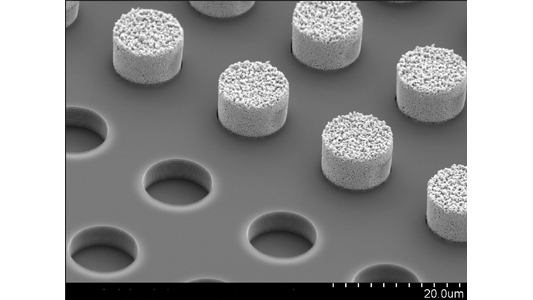
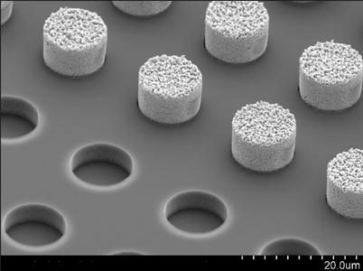
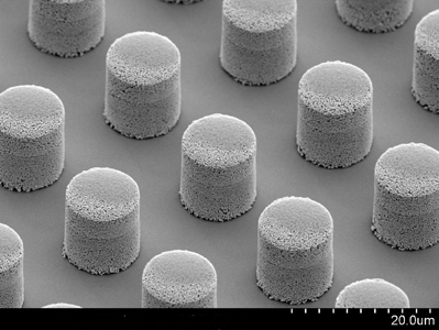
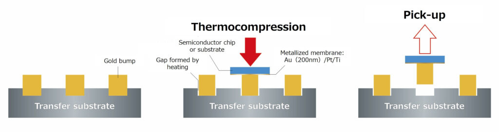
In this technology, at first, gold bumps are formed on a substrate (transfer substrate). Then, the gold bumps are transferred to the target semiconductor chip or substrate. Openings are created on the silicon substrate used as the transfer substrate, and gold bumps are formed in them. By filling the entire opening, the gold bump is held by the substrate, eliminating the risk of dropping during the process. Meanwhile, during transfer, the gold bump shrinks under heat-treatment, forming a tiny gap between the opening and the gold bump. This allows easy extraction of gold bumps by the application of a force in the vertical direction.
As the traditional gold bump formation process is a method that directly forms bumps on the target semiconductor chip or substrate, it is difficult to handle target chips and substrates with complex shapes, such as protrusions, dents, or open holes due to issues such as inconsistent resist heights.
In this current transfer technology, gold bumps are manufactured separately and can be transferred only to the target locations. This allows the technology to also be applied to complex shapes. It can also be used with semiconductor chips and substrates that are difficult to process using photolithography*3 due to concerns about damage from stripping solutions and others.
Manufacturing of transfer substrate and transfer and bonding process

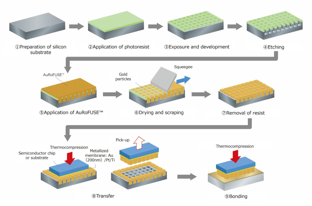
(1) Preparation of silicon substrate as transfer substrate
(2) Application of photoresist to silicon substrate
(3) Exposure and development of target pattern
(4) Etching of silicon substrate to create holes
(5) Application of AuRoFUSE™ using a squeegee, etc.
(6) Vacuum drying of AuRoFUSE™ at room temperature and scraping off excess gold particles on the resist
(7) Removal of resist to complete transfer substrate
(8) Placement of transfer substrate on target (semiconductor chip or substrate) for gold bump formation, thermocompression at 10 MPa and 150℃ for one minute, followed by vertical lifting of substrate to transfer gold bumps
(9) Bonding of post-transfer target through thermocompression at 20 MPa and 200℃ for 10 seconds
An illustration of the traditional gold bump formation process is available in the “Manufacturing of AuRoFUSE™ Preforms” section for reference on TANAKA’s website.
About the sintered gold bonding technology “AuRoFUSE™ Preforms”
Developed by TANAKA, “AuRoFUSE™ Preforms” is a bonding technology that forms bumps of all kinds of shapes using a paste comprising gold particles and an organic solvent. Through a thermocompression bonding process (20 MPa at 200℃ for 10 seconds), AuRoFUSE™ Preforms exhibits compression of approximately 10% in the compressive direction while showing minimal deformation in the horizontal direction. This gives them sufficient bonding strength*4 for practical applications. With the main component being gold, which has a high level of chemical stability, AuRoFUSE™ Preforms also provides excellent reliability after mounting.
This technology enables miniaturization of semiconductor wiring and greater integration (higher density) for various types of chips. It is expected to contribute to the needs for miniaturization and better performance of semiconductors, which have been rising in recent years, including optical devices such as light-emitting diodes (LEDs) and semiconductor lasers (LDs), use in digital devices such as personal computers, smartphones, as well as in-vehicle components, micro-electromechanical systems (MEMS), and such.
Traditionally, the main methods used in bump formation technology are soldering and plating. However, as solder tends to spread outward in molten state, there was the risk of short-circuiting through contact between electrodes as the bump pitch becomes finer. Meanwhile, plating can achieve a fine pitch, but because comparatively higher pressures are required during bonding, there is the possibility of causing chip damage. For reference, an illustration outlining the advantages of this technology compared with soldering and plating materials is provided in the “Comparison of AuRoFUSE™ Preforms with Other Materials” section on TANAKA’s website. This technology was developed to address these issues for use in next-generation high-density mounting and photonics-electronics integration devices.