
This technical article analyzes the design and performance of the EPCSC401 demonstration board, evaluating its radiation tolerance, thermal efficiency, and high-frequency switching topology.
Technological Context
Aerospace power system design faces a growing demand for power density and efficiency that exceeds the physical limits of traditional silicon MOSFETs, whose thermal losses and restricted switching frequencies heavily penalize payload weight.
Consequently, GaN technology emerges as a disruptive necessity for NewSpace architectures, thanks to its wider bandgap and superior electron mobility. The EPCSC401 demonstration board facilitates this transition, allowing engineers to evaluate synchronous GaN power stages under extreme radiation conditions.
System Architecture
The architectural foundation of the EPCSC401 demonstration board rests entirely on a synchronous buck converter topology, explicitly designed to mitigate switching and conduction losses in critical aerospace environments. The core of this power system comprises the synergistic integration of two critical semiconductor subcomponents: the EPCS4001 PWM controller and the EPC7011L7SH monolithic GaN power stage.
The EPCS4001 controller is an application-specific integrated circuit engineered using specialized CERN-developed technology. This ASIC delivers optimized gate drive signals, ensuring optimal timing and precise dead-time control. This highly responsive performance is fundamental to preventing shoot-through conduction between the high-side and low-side transistors, thereby maximizing the overall conversion efficiency of the power module. Moreover, it provides a full analog, voltage-mode control loop, which simplifies applications where tight output current control is not required. Finally, the controller has the infrastructure to efficiently power downstream power stages, either ar 12V or 5V.
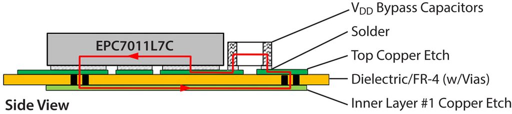
Complementing the IC, the EPC7011L7SH power stage houses high-reliability eGaN® FETs in a standard half-bridge configuration. By monolithic integration of the high-side and low-side field-effect transistors within a single, hermetic, surface-mount ceramic package, the loop inductance of the power circuit is drastically minimized and the gate drive loop is inherently optimal. This reduction in parasitic inductances successfully mitigates undamped oscillations at the switching nodes and completely eliminates the need for bulky snubber networks, directly optimizing the board’s final power density.
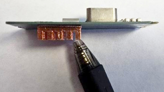
Furthermore, the physical PCB layout delivers high engineering versatility by enabling either conventional magnetic-core inductors or coreless inductors. This flexibility is vital for aerospace systems engineers to exercise trade-offs between component mass, volume constraints, electrical efficiency, and EMI profiles within the output filtering stage under strict space operating conditions. This structural combination ensures an optimal balance between reliability and high-speed electrical performance.
Electrical Performance and High-Frequency Switching
The electrical performance of the EPCSC401 demonstration board is meant to provide a baseline for power distribution networks in modern spacecraft, operating across a nominal input voltage range from 20 V to 50 V. The buck regulator circuit is optimized to power critical digital payloads and low-voltage subsystems, delivering a highly stable 12 V or 12.5 V output configuration that can be trimmed down to 3.3V, with a continuous current capability of up to 5 A.
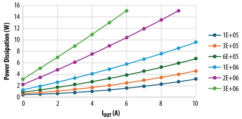
The primary operational advantage of this platform lies in its capability to operate high-frequency switching, within the range of 500 kHz and 3 MHz. This range is a perfect match forthe eGaN® FETs housed inside the EPC7011L7SH power stage module.
Unlike legacy silicon MOSFETs, gallium nitride devices exhibit zero reverse recovery charge (Qrr = 0). This unique material characteristic completely eliminates traditional body diode recovery losses during dynamic turn-on transitions, thereby minimizing thermal dissipation and boosting the overall conversion efficiency of the power converter.
Operating in the megahertz frequency spectrum allows systems engineers to drastically downsize the physical volume and mass of the passive filtering components, most notably the output inductor and the filtering capacitor bank. Furthermore, the multi-layer PCB layout is meticulously designed with adjacent ground planes to minimize the high-frequency current loop area. This precise geometric configuration successfully prevents parasitic inductive voltage spikes, dampens radiated EMI profiles, and ensures outstanding transient response along with optimal dynamic stability during sudden step-load variations on the power line.
Radiation Tolerance and Robustness
Radiation robustness within orbital environments is the single most critical factor for validating power components in aerospace missions, and the EPCSC401 platform is systematically engineered to mitigate these risks. Unlike traditional silicon MOSFETs, the eGaN® FETs embedded inside the EPC7011L7SH power stage possess a wide-bandgap gallium nitride crystal structure that intrinsically lacks a fragile gate oxide isolation layer.

The absence of this oxide eliminates charge trapping mechanisms within the dielectric material, effectively eradicating catastrophic failures caused by gate dielectric breakdown and severe shifts in threshold voltage parameters. Consequently, the GaN-based power stage demonstrates practical immunity to Total Ionizing Dose (TID), safely enduring accumulated radiation exposures exceeding 1 Mrad(Si) without suffering operational degradation.
Furthermore, the board delivers comprehensive protection against destructive Single-Event Effects (SEE) triggered by heavy ion strikes. The entire topology remains immune to Single-Event Burnout (SEB) and Single-Event Gate Rupture (SEGR) up to a high Linear Energy Transfer (LET) threshold of 84 MeV⋅ cm²/mg.
Complementing the power stage, the EPCS4001 ASIC gate controller, built upon radiation-hardened design architectures originally developed for CERN-level particle physics environments. This specialized silicon integrated circuit provides extreme magnetic field immunity, operating reliably in environments with magnetic fluxes exceeding 40,000 Gauss; TID and SEE ratings are met with a worst case 25% output voltage perturbation for Single Event Transients This eliminates the requirement for heavy shielding, potentially lowering overall satellite mass and directly reducing structural launch expenses.
Thermal Management and Mechanical Design
Heat dissipation and structural integrity present critical engineering hurdles within extreme space environments due to the complete absence of atmospheric convection inside an orbital vacuum. To overcome this limitation and prevent localized hotspots, the EPCSC401 demonstration board incorporates an advanced thermal management strategy that relies fundamentally on solid conductive heat transfer.
The EPC7011L7SH GaN power module is housed within a surface-mount ceramic package specifically designed with extremely low thermal resistance down to the PCB substrate. This allows the thermal energy generated at the transistor junctions to transfer directly and immediately into the internal heavy copper planes of the printed circuit board.
The physical design of the board utilizes a dense array of filled and plated thermal vias placed strategically directly beneath the power stage footprint. These vias act as low-impedance thermal bridges that route the heat flux vertically down to a secondary dissipation layer on the bottom side of the board, which can be mechanically coupled to an aluminum chassis or an external thermal radiator.
Conclusion
The EPCSC401 demonstration board conclusively validates the viability and structural advantages of eGaN® technology within aerospace power conversion systems. By successfully integrating the advanced EPCS4001 ASIC controller and the hermetic EPC7011L7SH power stage into a single compact platform, EPC Space provides flight systems engineers with a rigorous evaluation tool that bypasses the thermal, electrical, and frequency limitations of traditional silicon.
The effective mitigation of circuit parasitic inductances, combined with outstanding immunity against cosmic radiation and severe magnetic fields, establishes this power architecture as a fundamental building block for future generations of LEO and GEO satellite constellations, directly optimizing subsystem power density and accelerating critical space qualification testing timelines for modern aerospace missions.