

How Strategic Investments, Advanced Manufacturing, and Policy Reforms Are Positioning India at the Center of the Global Semiconductor Supply Chain
By: Editorial Team | Electronics Era
In today’s economy, semiconductors represent the basis of strategy. All modern smartphones, EVs, industrial robots, AI servers, medical technology, satellites, defense systems, and telecommunications infrastructure rely on ever more advanced integrated circuits. The growing adoption of Artificial Intelligence, 5G, Industry 4.0, autonomy in mobility and edge computing have increased the demand for semiconductors like never before.
Disruptions in the supply chain caused by the coronavirus outbreak and ensuing geopolitical tensions have changed the way that governments and industries perceive semiconductor production. From a purely commercial business, semiconductor production has become a question of economic resilience and national security. Governments in North America, Europe, East Asia, and the Middle East are pouring billions into building local semiconductor ecosystems and diversifying manufacturing capabilities.

In this regard, India has stepped into the race with renewed vigor. Apart from being known as one of the biggest semiconductor designs destinations in the world, India is also forming a comprehensive ecosystem involving everything from wafer fabrication and assembly to testing, advanced packaging, materials, equipment, research, and workforce development. The goal here is not only manufacturing of chips, but rather becoming a trustworthy partner in the global semiconductor value chain.
This process has been accelerated through various policy actions and investments in recent years. According to government forecasts, India’s semiconductor market that was worth roughly $38 billion in 2023 will grow to around $45-50 billion in 2024-2025 and will hit $100-110 billion in 2030 due to artificial intelligence, automotive electronics, consumer goods, industrial automation, and telecommunications.
A Global Industry Under Transformation
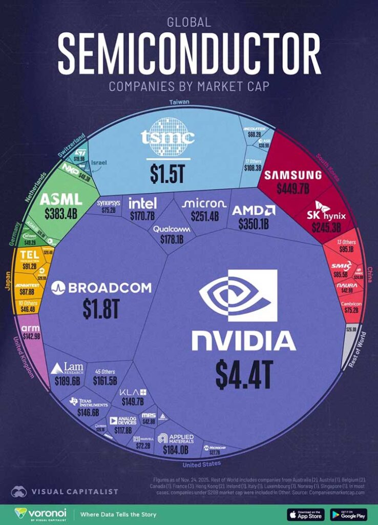
The global semiconductor industry is witnessing perhaps one of the biggest investment cycles ever in history. Artificial intelligence has spurred unprecedented demand for semiconductors such as processors, high-speed memory, networking semiconductors, and accelerators. Electric cars also need a lot more semiconductors compared to traditional vehicles, and technologies like 5G networks, smart factories, cloud computing, and IoT are expanding the market even further.
In addition, geopolitical uncertainties have brought out the dangers associated with too much reliance on geographic clusters in manufacturing processes. This is why governments globally are pushing for more regional manufacturing with the help of incentives, joint ventures, and research infrastructure.
India’s semiconductor strategy is highly aligned with this global trend. Instead of trying to challenge existing manufacturing leaders in each technological node, India is choosing to adopt a more phased approach which includes semiconductor designing, manufacturing, packaging, and supply chain localization.
India’s Existing Competitive Advantage
India is already at a unique position in the international semiconductor value chain.
Currently, hundreds of designers from India are actively involved in designing processors, communication semiconductors, automotive semiconductors, AI accelerators, power management semiconductors, RF front ends, and embedded system semiconductors used across the world. Some of the most notable semiconductor companies such as Intel, AMD, Qualcomm, Texas Instruments, NXP Semiconductors, Infineon Technologies, Micron Technology, Synopsys, Cadence, MediaTek, and Analog Devices have research and development centers in various cities of India, including Bengaluru, Hyderabad, Noida, Pune, Chennai, and Gurgaon.
The industry believes that almost twenty percent of all the semiconductor designers in the world hail from India, providing India a good base for developing manufacturing facilities.
Policy as the Growth Catalyst
India’s semiconductor plans are aided by what is probably one of the most ambitious industrial policy efforts made by India.
The India Semiconductor Mission (ISM), along with the PLI Scheme and DLI Scheme, as well as other electronics manufacturing initiatives, plans to develop a complete semiconductor ecosystem including:
- Wafer fabrication (fabs)
- Assembly, Testing, Marking, and Packaging (ATMP)
- Outsourced Semiconductor Assembly and Test (OSAT)
- Compound semiconductor fabrication
- Semiconductor design
- Display fabrication
- Research and development
- Talent development
The next phase of the government’s assistance efforts seems to be gaining momentum too. As late as in mid-June 2026, the Expenditure Finance Committee of the Finance Ministry cleared a plan for India Semiconductor Mission 2.0 which is expected to cost around ₹1.2-1.25 lakh crore, subject to approval from the Cabinet.
Beyond Fabs: Building the Complete Semiconductor Value Chain
Although semiconductor fabricating plants (fabs) form the core of semiconductor production, it should be noted that an ecosystem capable of competing in the global market of semiconductors reaches much farther than mere wafer production. The success of India in the long term would be contingent on the creation of an end-to-end value chain of Electronic Design Automation (EDA), IP, semiconductor materials, specialty chemicals, industrial gases, silicon wafers, photomasks, semiconductor manufacturing equipment, Assembly, Testing, Marking and Packaging (ATMP), Outsourced Semiconductor Assembly and Test (OSAT), advanced packaging, reliability testing and logistics. Specialists in the industry note that although fabs generate certain share of value in themselves, a robust supply chain and ecosystem players are just as important. Since ISM is placing more emphasis on ecosystem development along with fabrication, India will have every chance to build an independent semiconductor ecosystem based on its strengths in design, engineering and manufacturing.
Advanced Packaging: India’s Fastest Route to Global Leadership
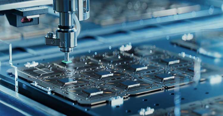
Whereas cutting-edge fabrication requires investment above US$10-20 billion, advanced packaging is a relatively quick and commercially attractive way in for India.
Advanced semiconductor technology is becoming increasingly reliant not just on transistor scaling but also on complex packaging.
They include such things as:
- SiP – System-in-Package
- FOWLP – Fan-Out Wafer-Level Packaging
- 2.5D Integration
- 3D Packaging
- TSV – Through-Silicon Via
- Chiplet Integration
- Heterogeneous Integration
With the advent of the AI revolution, chiplet-based architecture is being developed which can enable several specialized dies to work together as an integrated processor. Advanced packaging is thus emerging as one of the fastest-growing areas of semiconductor technology.
India’s efforts towards setting up OSAT and ATMP infrastructure put it in a strong position to capitalize on this market opportunity.
Compound Semiconductors Open New Opportunities
The emerging compounds of semiconductors, including Silicon Carbide (SiC), Gallium Nitride (GaN), and Gallium Arsenide (GaAs), are revolutionizing next generation electronics owing to their superior power efficiency, higher switching frequency, enhanced thermal characteristics, and higher power density relative to traditional silicon devices. Adoption of these semiconductors is taking off rapidly in the fields of electric vehicles (EV), renewable energy systems, 5G/6G infrastructures, aerospace and defense, automation industries, and fast charging. With respect to India, it is an advantageous move for India to develop local expertise in making these compounds of semiconductors considering that it is developing a robust electronic industry and semiconductor industry.
AI Is Reshaping Semiconductor Demand
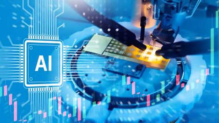
Artificial Intelligence is changing the manufacturing priorities for semiconductors.
Developing large language models and using AI systems necessitates specific hardware components such as GPUs, AI accelerators, high bandwidth memory, advanced networking chips, and packaging technology.
Future investments in semiconductor manufacturing will revolve around the following technologies:
- AI accelerators
- Edge AI processors
- Neural Processing Units (NPUs)
- High bandwidth memory
- Chiplets
- Photonic Interconnects
The convergence of the above technologies offers an opportunity for India to integrate its expertise in software, AI, semiconductors, and electronics.
Infrastructure: The Backbone of Semiconductor Manufacturing
Excellent infrastructure is a necessary component in setting up the manufacturing environment of semiconductors. Semiconductors manufacturing plants demand uninterrupted power supply, ultra-pure water (UPW), sophisticated waste management system, clean rooms, efficient logistics, and high speed internet connectivity to make sure of consistent production yield and efficiency in operation. Any disruption might disturb process stability and would raise manufacturing costs substantially. India is working on developing dedicated semiconductor clusters and corridors along with manufacturing parks that have dependable utilities and infrastructure. Along with development of better transport and port connectivity systems, along with sustainable energy options, this development would create an environment for manufacturing chips, semiconductor supply chain and advanced packaging, making India a manufacturing hub for the world.
Developing Domestic Supply Chains
A well-rounded set of suppliers is essential in semiconductor fabrication.
Future growth relies on domestic competence in:
- Speciality chemicals
- Industrial gases
- Precise ceramics
- Silicon wafers
- Quartz parts
- Vacuum technology
- Service of semiconductor equipment
- Automations software
- Facility consumables
Domestic suppliers will lower logistical costs, provide greater security, and offer opportunities to India’s MSMEs and technology start-ups.
Talent: India’s Strongest Asset
One of India’s biggest competitive advantages is in engineering skills.
Every year, a number of graduates are turned out from Indian universities specializing in electronics, electrical engineering, computer science, materials science, mechanical engineering, and manufacturing.
However, mastering manufacturing requires specific skill sets such as:
- Process engineering
- Lithography
- Yield engineering
- Device physics
- Packaging technology
- Reliability engineering
- Failure analysis
- Clean room
- Maintenance of equipment
This will be critical for developing such a workforce.
Sustainability in Future Semiconductor Manufacturing
Sustainability also needs to be considered when designing the semiconductor industry of today.
Future fab plants will need to consider:
- Integration of renewable energy
- Recycling of water
- Energy-efficient machinery
- Green chemistry
- Waste minimization
- Carbon management
- Sustainable manufacturing
By designing a sustainable semiconductor plant right from the start, it gives India an opportunity to meet the changing global standards of sustainability.
Research, Innovation and Strategic Partnerships
Competitiveness is built through innovations continuously.
Some of the areas of research focus in India today are:
- Silicon Photonics
- MEMS
- QD devices
- Package innovations
- WBG Semiconductors
- Hardware for AI
- Power Electronics
- Semiconductor reliability
- Automation in manufacturing
The level of collaboration between universities, research labs, startups, international technology companies, and manufacturing companies will define how fast India progresses in these areas.
There are also some international partnerships in action.
Some more recent partnerships have been announced by leading semiconductor firms who have continued to engage themselves with India’s ecosystem through partnerships in packaging, manufacturing, and technology development such as Infineon.
Market Outlook
Several industry predictions suggest continued growth.
According to government and industry projections, Indian demand for semiconductors may rise to over US$100 billion by 2030, while third-party market research predicts robust double-digit growth due to artificial intelligence, electric mobility, industrial automation, telecoms, and consumer electronics.
Nevertheless, the policy environment is becoming increasingly favorable. The launch of new initiatives in the context of India Semiconductor Mission 2.0, greater investments in semiconductor infrastructure, more international collaboration, and active engagement in the global semiconductor value chain reveal that the aspirations of India in the semiconductor sector are shifting from policy pronouncements to actual implementation.
Conclusion
India is at a pivotal point in its semiconductor development, moving from a focus on design and engineering to building a comprehensive manufacturing ecosystem. Success will rely on investments in infrastructure, supply chains, research, and international collaboration. As demand grows in sectors like AI and telecommunications, India aims to shift from being a mere consumer of semiconductor technology to a competitive global manufacturing leader, enhancing both national self-reliance and the global supply chain’s resilience over the next decade.