

By: Mr. Sudhir Naik, Semiconductor man of Gujarat, IESA Executive Director & Treasure, Dr. Vandana Shah, Associate Professor, Sarvajanik University
Semiconductor technology is exceptionally complex, as it manipulates matter at the atomic level and requires a highly sophisticated, globally interconnected ecosystem. Although semiconductor transistors have been commercially produced for decades, no single company or nation can independently manufacture advanced semiconductor chips without relying on global partners, technologies, equipment, materials, and supply chains. The enormous cost of establishing a semiconductor fabrication facility (FAB), often involving multibillion-dollar investments, further highlights the complexity of the industry. Returns on investment take several years, while rapid technological advancement and stringent yield requirements add significant business and technical challenges.
The recent advancement toward sub-nanometer semiconductor technology, with companies such as TSMC and Samsung leading the field while Intel continues to pursue similar capabilities, demonstrates the enormous R&D effort required to establish and operate world-class FABs.
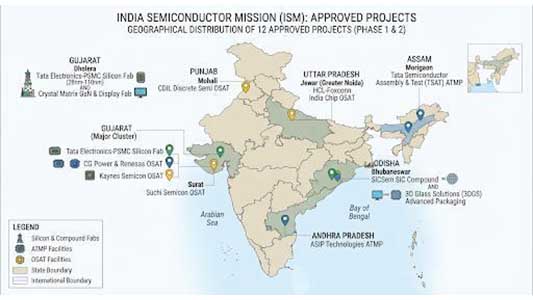
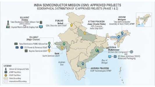
The map highlights the geographical distribution of projects approved under the India Semiconductor Mission (ISM) across key states, covering semiconductor fabs, ATMP/OSAT facilities and related projects.
These projects mark India’s growing semiconductor manufacturing ecosystem, with Gujarat, Assam, Odisha, Uttar Pradesh and Andhra Pradesh emerging as important semiconductor hubs. Under the leadership of the Government of India, the India Semiconductor Mission (ISM) was established in 2022 with an initial outlay of approximately ₹76,000 crore. Similar government-supported initiatives exist in the USA, Europe, Japan and other countries because semiconductor manufacturing is highly capital-intensive and strategically important. The ISM framework provides substantial financial support for semiconductor projects, complemented by additional support from state governments. The ISM policy supports up to 50% Investment by any organisation and State government support varies from 25% to 30% on Peri Passu basis.
India has already made significant progress in semiconductor assembly and packaging. Micron US based company ,which makes memory chips was the anchor company to show trust in Indian talent and Micron CEO Mr Sanjay Mehrotra ( Indian Origin) signed an MoU with the Government of Gujarat in June 2023 for an OSAT facility in Sanand. The facility, inaugurated in February 2026, represents an estimated investment of approximately ₹22,516 crore (US$2.75 billion) and is expected to reach a peak capacity of around 1.35 billion chips annually. Other major OSAT projects include Kayens Semicon and CG Power in Gujarat, while Tata has announced a major semiconductor facility in Assam.
A landmark development is Tata Group’s proposed semiconductor FAB at Dholera, Gujarat, with an investment of approximately US$11 billion. The proposed facility will manufacture chips across the 28 nm to 110 nm technology nodes, with Taiwan’s PSMC (Powerchip Semiconductor Manufacturing Corporation) identified as the technology partner. These developments represent important steps toward establishing India’s semiconductor manufacturing foundation.
However, building a FAB is only one part of the semiconductor journey. Semiconductor production depends on a complex global supply chain involving silicon, specialty chemicals, gases, equipment, engineering services, rare-earth materials, packaging technologies and other critical inputs. The journey from raw materials to a finished semiconductor can cross multiple countries and thousands of kilometres before the final chip reaches the consumer.
Therefore, the next phase of India’s semiconductor strategy focuses on strengthening the broader supply chain and developing skilled human resources. ISM 2.0 is intended to expand the ecosystem from chip design and IP creation through manufacturing, packaging, components and supporting materials. The objective is to increase domestic semiconductor and electronics manufacturing capacity and reduce India’s dependence on imports.
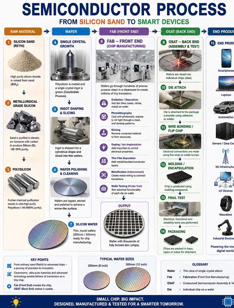
The diagram illustrates the complete semiconductor manufacturing journey, from silicon sand and purification to wafer fabrication, chip manufacturing, assembly, packaging, and final testing. It highlights how FAB (front-end manufacturing) creates the semiconductor devices, while OSAT (back-end manufacturing) performs dicing, assembly, bonding, packaging, and testing before the chips are integrated into smart devices and systems.

India currently has a major advantage in semiconductor chip design. Approximately 1.5 lakh engineers are engaged in semiconductor design activities, and most leading global semiconductor companies have significant R&D operations in India. The strategic priority is therefore to complement India’s existing design strength with domestic manufacturing, packaging, testing and supporting ecosystems.
Several semiconductor projects are already progressing, with some facilities entering commercial production while others are expected to become operational during 2027–28. Locations such as Dholera, Bhubaneswar, Visakhapatnam and Uttar Pradesh are emerging as important semiconductor hubs, with Dholera expected to become a major centre for India’s semiconductor manufacturing ambitions.
Overall, India’s semiconductor journey is not simply about building a FAB. It is about creating an end-to-end ecosystem—from chip design and IP to fabrication, packaging, testing, materials, equipment, skilled manpower and supporting industries. The ambition to establish India’s first FAB and develop a globally competitive semiconductor ecosystem marks a significant step toward strengthening India’s technological and strategic self-reliance.
Dholera SIR will be the epicentre of India’s semiconductor manufacturing movement, with all the essential pillars required to accommodate several FABs. Spread across approximately 940 sq. km, one of the largest land parcels in Asia, Dholera offers an international airport within 40 km, high-speed road and rail connectivity to Ahmedabad, and, most importantly, reliable water and power infrastructure. Semiconductor FABs require millions of gallons of continuous water supply, which is supported through a dedicated Narmada canal and a completed water-conservation project. Equally critical is stable, uninterrupted power, supported by the electricity grid and a massive operational solar plant. With land, water, power and connectivity infrastructure in place, Dholera is uniquely positioned to emerge as India’s semiconductor manufacturing hub, while cities such as Bhubaneswar and others may replicate this model in the coming years.